

Microled display panel
a display panel and micro-lead technology, applied in static indicating devices, instruments, electroluminescent light sources, etc., can solve the problems of thermal mismatch, significant impact, and complex flip chip technology, and achieve the effect of reducing the loading of drivers
- Summary
- Abstract
- Description
- Claims
- Application Information
AI Technical Summary
Benefits of technology
Problems solved by technology
Method used
Image

Examples
Embodiment Construction
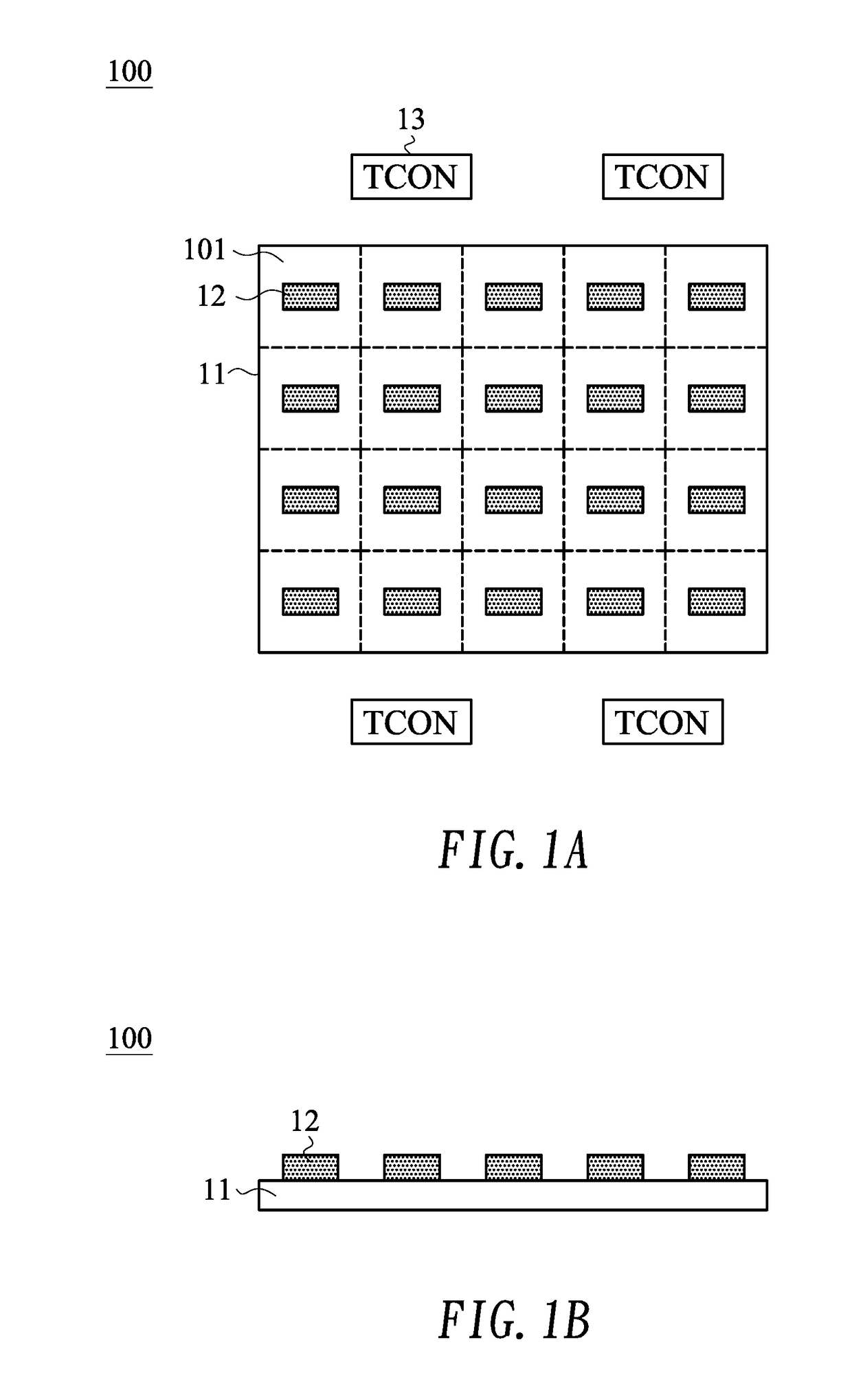
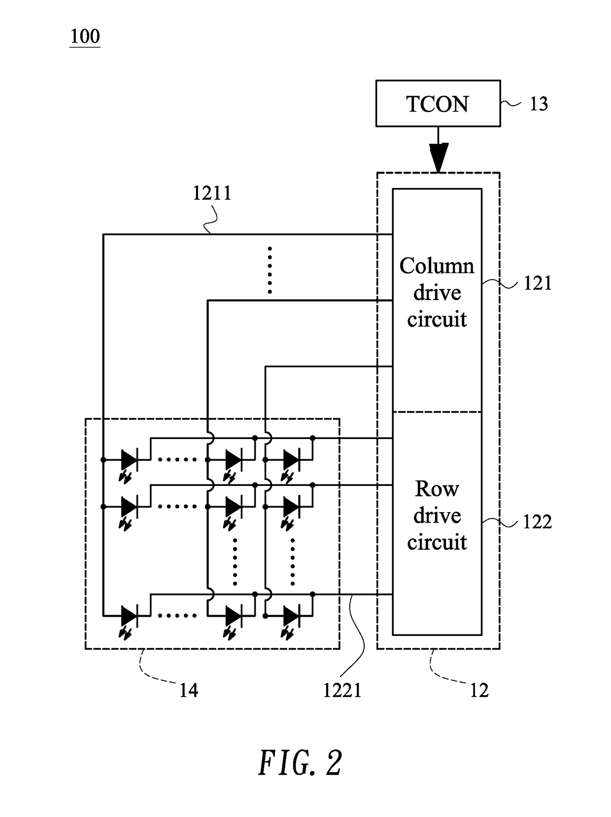
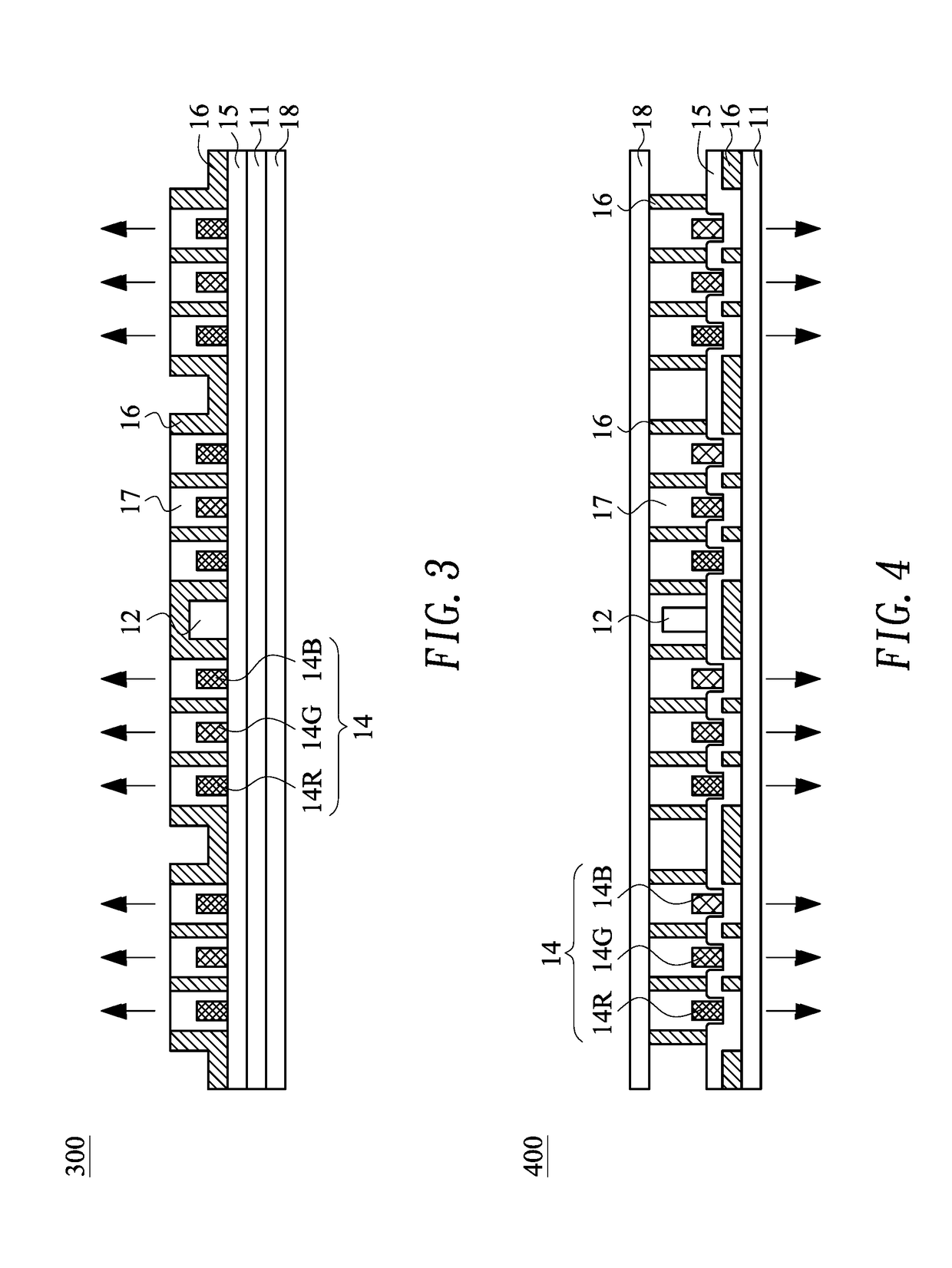
[0023]FIG. 1A shows a top view illustrated of a micro light-emitting diode (microLED) display panel 100 according to one embodiment of the present invention, and FIG. 1B shows a side view illustrated of the microLED display panel 100 of FIG. 1A. The microLED display panel of the embodiment is preferably adaptable to a large-size and high-resolution (e.g., 3840RGB×2160) display panel. In the specification, the size range of the microLED is between 1 and 10 micrometers. However, the size of the microLED may be even smaller due to specific applications or technological advance. In the specification, “large-size” display panel is currently and commonly referred to 10 inches or above display panel. However, “large-size” display panel may be referred to other display size due to specific applications or technological advance. In the specification, “high-resolution” display panel is currently and commonly referred to a display panel with 1080 or above scan lines. However, “high-resolution”...
PUM
 Abstract
Description
Claims
Application Information