Optical phase modulator with sinusoidal pn junction

a technology of optical phase modulator and sinusoidal pn junction, which is applied in the field of optics and optoelectronics, can solve the problems of limited performance of such a modulator, and achieve the effects of reducing the length of the guide, in the main direction, and improving the amount of overlapping

Inactive Publication Date: 2019-01-17
COMMISSARIAT A LENERGIE ATOMIQUE ET AUX ENERGIES ALTERNATIVES
View PDF0 Cites 2 Cited by
  • Summary
  • Abstract
  • Description
  • Claims
  • Application Information

AI Technical Summary

Benefits of technology

[0021]This arrangement provides an improved amount of overlapping between the ZCE and the light flow. The phase shift obtained by the modulation is thus greater, and the modulator becomes particularly efficient.
[0023]With the solution claimed, since the amount of overlapping is improved, the length of the guide, in its main direction, can be reduced. This allows the bandwidth and thus the quickness of the modulator to be significantly increased. This also allows the control electronics to be simplified by using a single contact that is faster and simpler than a “traveling wave” contact for which differences in optical and electrical delays over a plurality of portions must be managed, for example.
[0024]Moreover, since the amount of overlapping is improved, it is not necessary to highly dope the P and N zones, thus reducing the optical losses.
[0025]Moreover, the solutions of the prior art mentioned above are not well suited to phase modulation in a multimode guide. The solution according to the invention allows the phase modulation in a multimode guide to be improved considerably, by voluntarily exciting various modes in this guide in such a way as to obtain a light flow having an optical power distribution according to an oscillating continuous function.
[0027]Moreover, the modulator according to the invention can have a width, i.e., a dimension in a direction perpendicular to the main direction, that remains limited. This small width contributes to reducing the time for the carriers to cross the PN Junction. Finally, this allows the quickness of the modulator to be improved even more.
[0030]The dimensional constraints associated with creating such a PN junction are advantageously relaxed and sufficiently low, in such a way that the creation of the PN junction can be carried out with the conventional techniques of lithography. The modulator according to the invention can thus be obtained in an easy, reproducible and not very costly way.

Problems solved by technology

However, the performance of such a modulator remains limited.

Method used


Image

  • Optical phase modulator with sinusoidal pn junction
  • Optical phase modulator with sinusoidal pn junction
  • Optical phase modulator with sinusoidal pn junction

Examples


Embodiment Construction

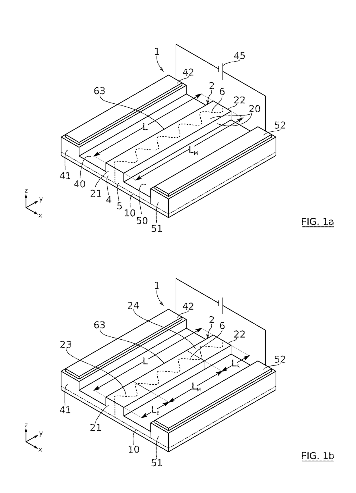
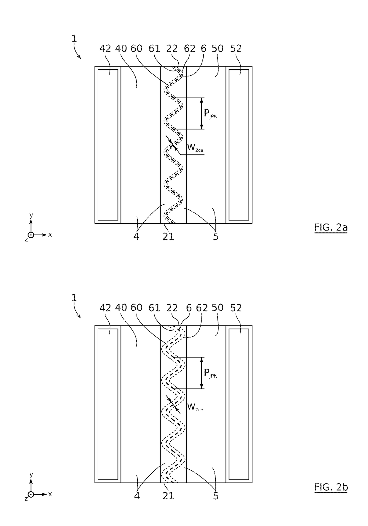
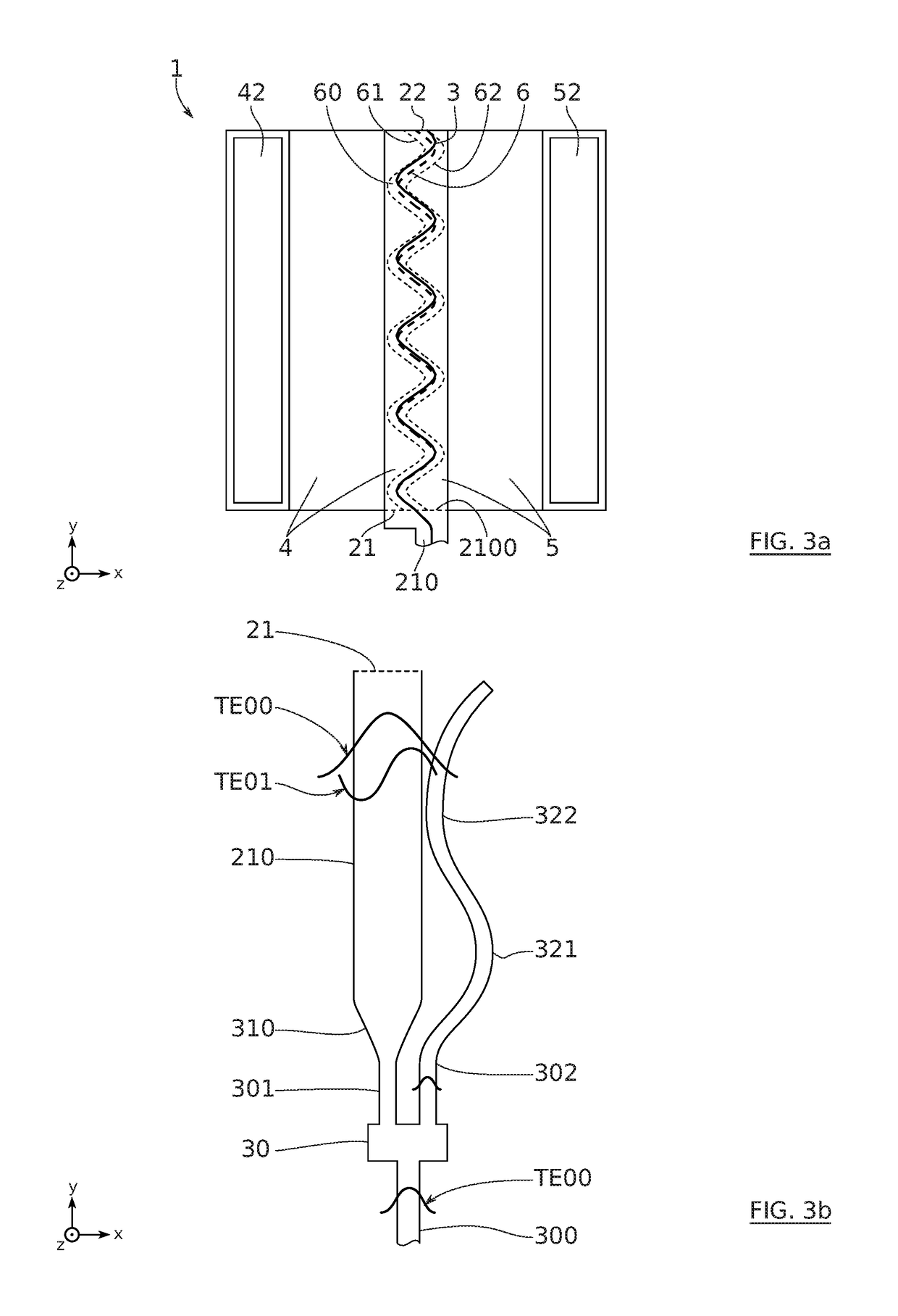
[0054]Before starting a detailed review of embodiments of the invention, optional features that can optionally be used in combination or alternatively are mentioned below:[0055]the oscillating continuous function is defined in such a way that the PN junction covers at least X % of the fight flow between the input and the output of the modulation guide, with X≥50, preferably X≥60, preferably X≥70, preferably X≥80, preferably X≥90.[0056]the oscillating continuous function forms oscillations each defining a crest and the crests of two successive oscillations are separated by a distance PjPNPjPN can thus be qualified as a peak-to-peak distance in the case in which the crests form peaks.[0057]the distance PjPN corresponds to the shortest distance between two successive crests taken from all of the crests formed by the PN junction along the modulation guide. Preferably, PjPN is such that PjPN≥300 nm, preferably PjPN≥750 nm, and preferably PjPN≥1 μm. This distance PjPN can be measured rega...


PUM

PropertyMeasurementUnit
wavelengthaaaaaaaaaa

Abstract

The object of the invention is a phase modulator including a modulation guide intended to guide die propagation of a light flow, said guide comprising a PN junction extending mainly along the main axis of propagation according to an oscillating continuous function. Advantageously, the oscillating continuous function is defined in such a way that the PN junction covers at least 50% of the light flow between the input and the output of the modulation guide. According to one possibility, the continuous function is sinusoidal. The object of the invention is also a switch and an intensity modulator each comprising a phase modulator.

Description

TECHNICAL FIELD OF THE INVENTION[0001]The invention relates to the field of photonics and optoelectronics. It has at least one particularly advantageous use in the field of modulators of optical signals. It has an advantageous but non-limiting use in the manufacturing of optical switches and intensity modulators, for example in the field of telecommunications.PRIOR ART[0002]There are several types of modulators for optical signals, in particular on a silicon chip. The modulation can be carried out either directly on the laser source, or by a dedicated electrooptical component in the circuit. Among these solutions, electrooptical modulators allow a greater bandwidth and a much higher modulation index than with direct modulation to be obtained. These components in particular allow throughputs greater than 25 Gb / s and / or modulation frequencies greater than 25 GHz to be reached.[0003]Among these components, phase modulators have the advantage of accepting relatively high optical powers,...

Claims


Application Information

Patent Timeline
Patent Type & Authority Applications(United States)
IPC IPC(8): G02F1/017G02F1/025
CPCG02F1/01708G02F2202/06G02F1/025G02F1/2257G02F1/0175
Inventor HASSAN, KARIMBOUTAMI, SALIMANFRAY, THOMAS
Owner COMMISSARIAT A LENERGIE ATOMIQUE ET AUX ENERGIES ALTERNATIVES
Why Eureka
Try Eureka