3D NAND array with divided string architecture

a technology of nand array and divided string, applied in the field of memory and storage devices, can solve the problems of large amount of power consumption, information stored in dram will eventually degrade, and nvm memory devices are more expensive but consume less power, so as to achieve the effect of not increasing the risk of program disturban

Active Publication Date: 2019-01-24
HSU FU CHANG
View PDF2 Cites 1 Cited by
  • Summary
  • Abstract
  • Description
  • Claims
  • Application Information

AI Technical Summary

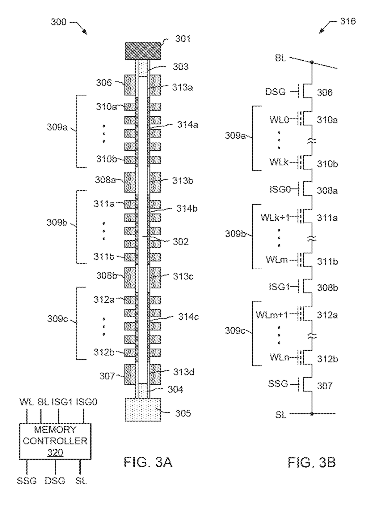
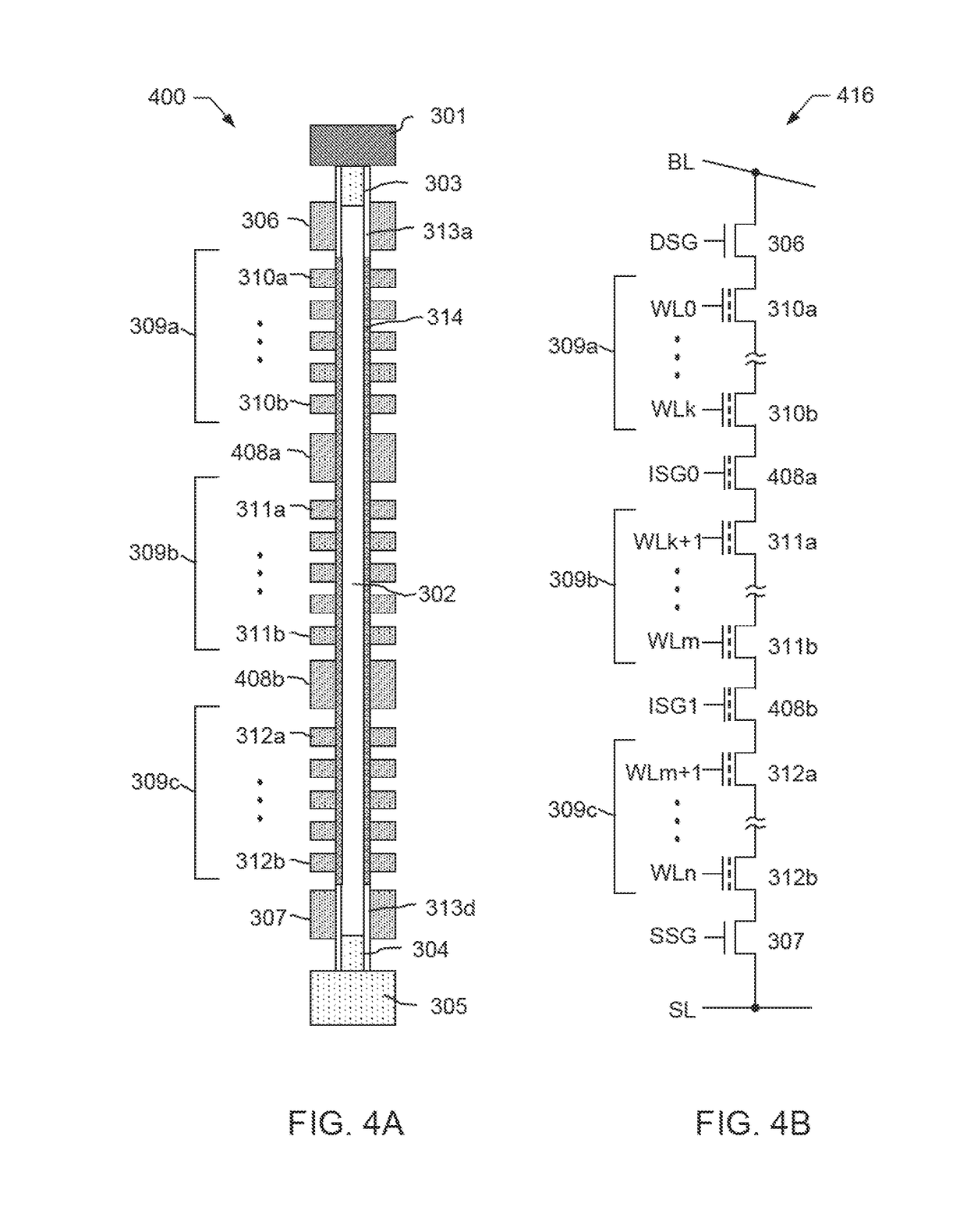
Benefits of technology

[0010]A novel 3D NAND array with divided string architecture is disclosed to address the issue of program-disturb in 3D memory arrays. In various exemplary embodiments, the divided string architecture enables more layers to be stacked in a 3D array without increasing the risk of program-disturb.
[0011]In various exemplary embodiments, the divided string architecture includes internal select gates within the cell string that divide the cell string into segments. Each segment contains a selected number of memory cells. During programming, the internal select gates can be enabled or disabled to isolate selected segments of the cell string. When programming an isolated segment, the problem of program-disturb for the remaining segments is reduced or eliminated. Thus, even with memory cell strings having many layers, the effects of program-disturb can be mitigated. In addition to the novel cell structure, several novel programming bias conditions are disclosed that allow programming of cells in one or multiple segments while reducing or eliminating the effects of program-disturb on the remaining segments of the cell string.

Problems solved by technology

Unfortunately, due to the dynamic nature of its configuration, the information stored in DRAM will eventually degrade unless periodic memory refresh cycles are performed.
Thus, though DRAM memory cells may be small in size, they may also consume large amounts of power due to the refresh requirements.
In contrast to DRAM, NVM memory devices maybe more expensive but consume less power.
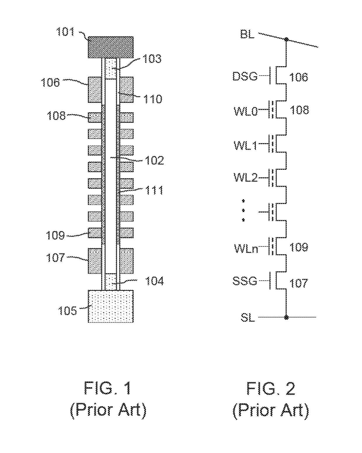
One significant drawback of conventional 3D NAND array structures that utilize the architecture of the cell string 100 is that of “program-disturb.” During programming, a selected word line (e.g., WL0) is supplied with a high voltage, such as +10V to +20V.
However, this condition will cause significant program-disturb to some or all of the cells associated with the unselected word lines.
Furthermore, as the density of the 3D NAND array is increased, more word line layers will be stacked in one string, and thus the problem of program-disturb is increased.
This problem will become even more severe for Multi-Level Cell (MLC) configurations because each level has a narrower voltage threshold (Vt) window.
Thus, the program-disturb problem has become a technical challenge for increasing the density of 3D NAND memory.

Method used


Image

  • 3D NAND array with divided string architecture
  • 3D NAND array with divided string architecture
  • 3D NAND array with divided string architecture

Examples


Embodiment Construction

[0027]Exemplary embodiments of the present invention are described herein in the context of a process, device, method, and apparatus for providing a novel dual function hybrid memory cell.

[0028]Those of ordinary skilled in the art will realize that the following detailed description is illustrative only and is not intended to be in any way limiting. Other embodiments of the present invention will readily suggest themselves to skilled persons having the benefit of this disclosure. Reference will now be made in detail to implementations of the exemplary embodiments of the present invention as illustrated in the accompanying drawings. The same reference indicators or numbers will be used throughout the drawings and the following detailed description to refer to the same or like parts.

[0029]It should be noted that the exemplary embodiments are not limited to ONO cells only and the disclosed aspects can be applied to other types of charge-trapping cells. To realize the low-cost, high-fle...


PUM


Abstract

A 3D NAND array with divided string architecture. In one aspect, an apparatus includes a plurality of charge storing devices connected to form a cell string. The apparatus also includes one or more internal select gates connected between selected charge storing devices in the cell string. The one or more internal select gates divide the cell string into two or more segments of charge storing devices. Selectively enabling and disabling the one or more internal select gates during programming operates to isolate one or more selected segments to reduce program-disturb to remaining segments. In another embodiment, a method is provided for programming a memory cell of a cell string having internal select gates that isolate the memory cell to reduce the effects of program-disturb. In another embodiment, multiple memory cells of a cell string having internal select gates are programmed with reduced program-disturb.

Description

PRIORITY[0001]This application is a divisional of a U.S. patent application having application Ser. No. 15 / 348,869, filed on Nov. 10, 2016, and entitled “3D NAND ARRAY WITH DIVIDED STRING ARCHITECTURE,” which further claims the benefit of priority based upon U.S. Provisional patent application having Application No. 62 / 253,683, filed on Nov. 11, 2015, and entitled “3D NAND ARRAY WITH DIVIDED STRING ARCHITECTURE,” all of which are hereby incorporated herein by reference in their entirety.FIELD OF THE INVENTION[0002]The exemplary embodiments of the present invention relate generally to the field of semiconductors and integrated circuits, and more specifically to memory and storage devices.BACKGROUND OF THE INVENTION[0003]Memory devices are widely used in a variety of digital electronics. One type of memory device is a dynamic random access memory (DRAM) device. DRAM devices can be used to form low cost high density memory arrays. For example, one of the largest applications for DRAM i...

Claims


Application Information

Patent Timeline
Patent Type & Authority Applications(United States)
IPC IPC(8): G11C16/34H01L49/02H01L27/1157G11C16/04G11C16/10H01L27/11524
CPCH01L28/00G11C16/0466H01L27/1157G11C16/04G11C16/3427G11C16/10H01L27/11524H10B41/35H10B43/35
Inventor HSU, FU-CHANG
Owner HSU FU CHANG
Why Eureka
Try Eureka