Member for semiconductor manufacturing device

a manufacturing device and semiconductor technology, applied in the direction of electrical discharge tubes, pressure inorganic powder coating, electrical apparatus, etc., can solve the problems of insufficient durability and cracking, and achieve the effect of suppressing the width of the concave and reducing the number of particles

Active Publication Date: 2019-01-24
TOTO LTD
View PDF0 Cites 3 Cited by
  • Summary
  • Abstract
  • Description
  • Claims
  • Application Information

AI Technical Summary

Benefits of technology

[0019]According to the member for the semiconductor manufacturing device, a width of the concavity can be suppressed from changing rapidly, and the stress generated near the interface of the first layer in t...

Problems solved by technology

However, cracking and peeling may occur in t...

Method used


Image

  • Member for semiconductor manufacturing device
  • Member for semiconductor manufacturing device
  • Member for semiconductor manufacturing device

Examples


Embodiment Construction

[0052]Various embodiments of the invention will be described hereinafter with reference to the accompanying drawings. In the drawings, similar components are marked with like reference numerals, and a detailed description is omitted as appropriate.

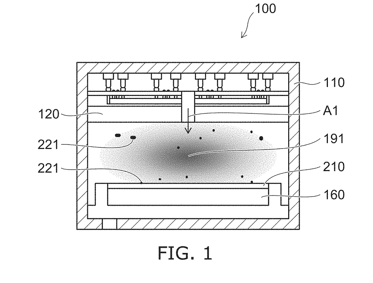
[0053]FIG. 1 is a cross-sectional view illustrating a semiconductor manufacturing device including a member for a semiconductor manufacturing device according to an embodiment.

[0054]A semiconductor manufacturing device 100 shown in FIG. 1 includes a chamber 110, a member for the semiconductor manufacturing device 120, and an electrostatic chuck 160. The member for the semiconductor manufacturing device 120 is called as a top board or the like, for example, and is provided in an upper portion inside the chamber 110. The electrostatic chuck 160 is provided in a lower portion inside the chamber 110. That is, the member for the semiconductor manufacturing device 120 is provided on the electrostatic chuck 160 inside the chamber 110. An object t...


PUM

PropertyMeasurementUnit
Fractionaaaaaaaaaa
Fractionaaaaaaaaaa
Fractionaaaaaaaaaa

Abstract

According to one embodiment, a member for a semiconductor manufacturing device includes an alumite base material including a concavity, and a first layer formed on the alumite base material and including an yttrium compound. The first layer includes a first region, and a second region provided in the concavity and located between the first region and the alumite base material. An average particle diameter in the first region is shorter than an average particle diameter in the second region.

Description

CROSS-REFERENCE TO RELATED APPLICATIONS[0001]This is a continuation application of International Application PCT / JP2017 / 032851, filed on Sep. 12, 2017. This application is also based upon and claims the benefit of priority from Japanese Patent Application No. 2016-178671, filed on Sep. 13, 2016, and Japanese Patent Application No. 2017-173746, filed on Sep. 11, 2017; the entire contents of which are incorporated herein by reference.FIELD OF THE INVENTION[0002]Aspects of the invention relate generally to a member for a semiconductor manufacturing device.BACKGROUND OF THE INVENTION[0003]A semiconductor manufacturing device is used for processing such as dry etching, sputtering and CVD (Chemical Vapor Deposition) or the like in a chamber in a manufacturing process of a semiconductor device. In this chamber, particles may be generated from a workpiece or an inner wall of the chamber or the like. Since the particles cause decrease of yield of the manufactured semiconductor device, the pa...

Claims


Application Information

Patent Timeline
IPC IPC(8): H01J37/32
CPCH01J37/32495H01J2237/0213C23C24/04H01L21/3065H01L21/67178H01L21/6719H01L21/6833H01L21/6835
Inventor NITTA, YASUTAKA
Owner TOTO LTD
Why Eureka
Try Eureka