
OLED flexible display panel and method for manufacturing the same

a flexible display panel and flexible technology, applied in the field of flexible display panels, can solve the problems of increasing the thickness of inorganic film, affecting the production efficiency of organic semiconductor devices, and difficult bending of inorganic films, etc., and achieves the effect of difficult cracking or peeling

Active Publication Date: 2019-01-31
WUHAN CHINA STAR OPTOELECTRONICS SEMICON DISPLAY TECH CO LTD
View PDF3 Cites 8 Cited by
  • Summary
  • Abstract
  • Description
  • Claims
  • Application Information

AI Technical Summary

Benefits of technology

This patent is about a new OLED flexible display panel and a method for making it. The panel has a layered structure that blocks water and oxygen, which can cause damage to the panel. This layered structure prevents the inorganic film in the panel from cracking or peeling during bending, which was a problem in previous designs. Overall, this patent solves the issue of vulnerability in OLED flexible display panels during bending.

Problems solved by technology

Inorganic films are dense, and inorganic films are difficult to bend because of generation of film stress during deposition.
Thus, inorganic film is liable to crack and peel.
However, increase of thickness of inorganic film would aggravate likelihood of occurrence of cracking and peeling.
In particular, for OLED flexible display panels, once the OLED flexible display panels are bended or folded, it is very likely that the inorganic film would experience cracking or peeling, causing failure of the OLED flexible display panels in devices.

Method used


Image

  • OLED flexible display panel and method for manufacturing the same
  • OLED flexible display panel and method for manufacturing the same

Examples


Embodiment Construction

[0057]The following provides clear and complete description of the embodiments with reference to the appended drawings. However, the described embodiments are just part, rather than all, of embodiments of the present disclosure. Any other embodiments obtained by those of ordinary skill in the art based on the embodiments of the present disclosure are intended to be protected by the subject invention.

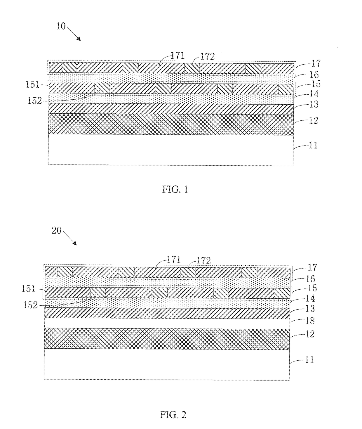
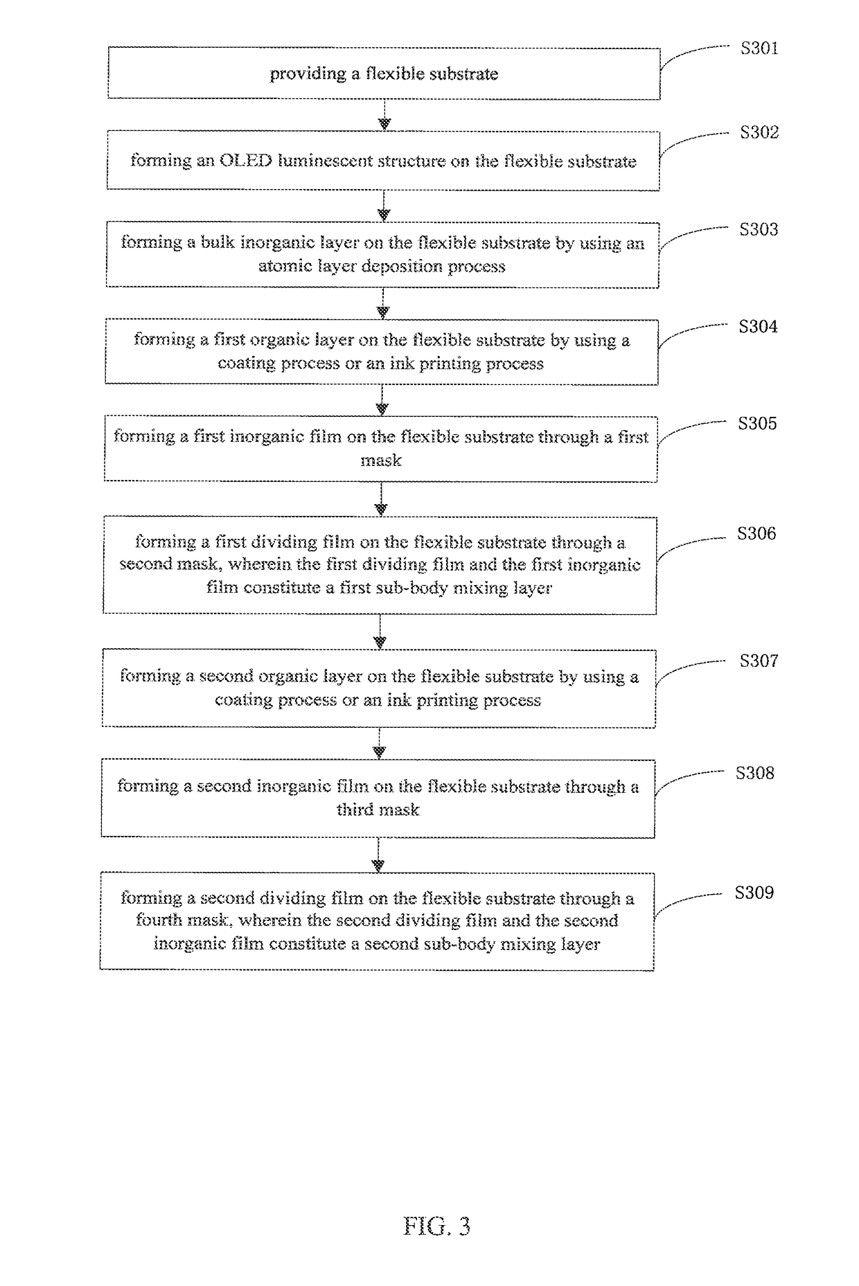
[0058]Please refer to FIG. 1, which is a schematic diagram showing a structure of an OLED flexible display panel according to a first preferred embodiment of the present disclosure. The organic light-emitting diode (OLED) 10 according to this preferred embodiment includes a flexible substrate 11, an OLED luminescent structure 12, a bulk inorganic layer 13, a first organic layer 14, a first sub-body mixing layer 15, a second organic layer 16, and a second sub-body mixing layer 17.

[0059]The OLED luminescent structure 12 is disposed on the flexible substrate 11. The bulk inorganic layer 13 ...


PUM

PropertyMeasurementUnit
thicknessaaaaaaaaaa
thicknessaaaaaaaaaa
thicknessaaaaaaaaaa

Abstract

The present disclosure provides an organic light-emitting diode (OLED) flexible display panel, comprising a flexible substrate, an OLED luminescent structure, a bulk inorganic layer, a first organic layer, a first sub-body mixing layer, a second organic layer, and a second sub-body mixing layer. The first sub-body mixing layer includes a first inorganic film and a first dividing film that are alternately arranged, and the second sub-body mixing layer includes a second inorganic film and a second dividing film that are alternately arranged.

Description

FIELD OF THE DISCLOSURE[0001]The present disclosure relates to the field of flexible display panel, and more particularly to an organic light-emitting diode (OLED) flexible display panel and a method for manufacturing the same.BACKGROUND[0002]Currently, organic light-emitting diode (OLED) display panels are encapsulated by a film, where the encapsulation film is a multi-layer inorganic film or a mutli-layer composed of alternating layers of deposited inorganic films and organic films. Inorganic films are dense, and inorganic films are difficult to bend because of generation of film stress during deposition. Thus, inorganic film is liable to crack and peel.[0003]In addition, to prevent water and oxygen from penetrating into OLED display panels, inorganic films are required to have a certain degree of thickness to block water and oxygen. However, increase of thickness of inorganic film would aggravate likelihood of occurrence of cracking and peeling. In particular, for OLED flexible d...

Claims


Application Information

Patent Timeline
Patent Type & Authority Applications(United States)
IPC IPC(8): H01L51/52H01L51/00H01L51/56
CPCH01L2251/303H01L51/56H01L2251/301H01L51/0097H01L2251/5338H01L51/5256H10K71/00H10K59/8731Y02E10/549Y02P70/50H10K77/111H10K2102/311H10K50/8445H10K2102/00
Inventor TANG, FAN
Owner WUHAN CHINA STAR OPTOELECTRONICS SEMICON DISPLAY TECH CO LTD
Learn More