Three dimensional chip structure implementing machine trained network

Active Publication Date: 2019-02-07
XCELSIS CORP
View PDF0 Cites 27 Cited by
  • Summary
  • Abstract
  • Description
  • Claims
  • Application Information

AI Technical Summary

Benefits of technology

[0005]Each latch in some embodiments is associated with one pair of boundary nodes, with one node in the first bonded layer and another node in the second bonded layer. Each pair of nodes is electrically interconnected through a conductive interface, such as a through-silicon via (TSV) or a direct bond interface (DBI) connection (also called hybrid bonding). Each latch in some embodiments is defined on just one of the two bonded layers. In some embodiments, each latch on one bonded layer has its output carried to the other bonded layer by interconnect (e.g., wires) an

Problems solved by technology

However, there has not been as much advances in c

Method used


Image

  • Three dimensional chip structure implementing machine trained network
  • Three dimensional chip structure implementing machine trained network
  • Three dimensional chip structure implementing machine trained network

Examples


Embodiment Construction

[0035]In the following detailed description of the invention, numerous details, examples, and embodiments of the invention are set forth and described. However, it will be clear and apparent to one skilled in the art that the invention is not limited to the embodiments set forth and that the invention may be practiced without some of the specific details and examples discussed.

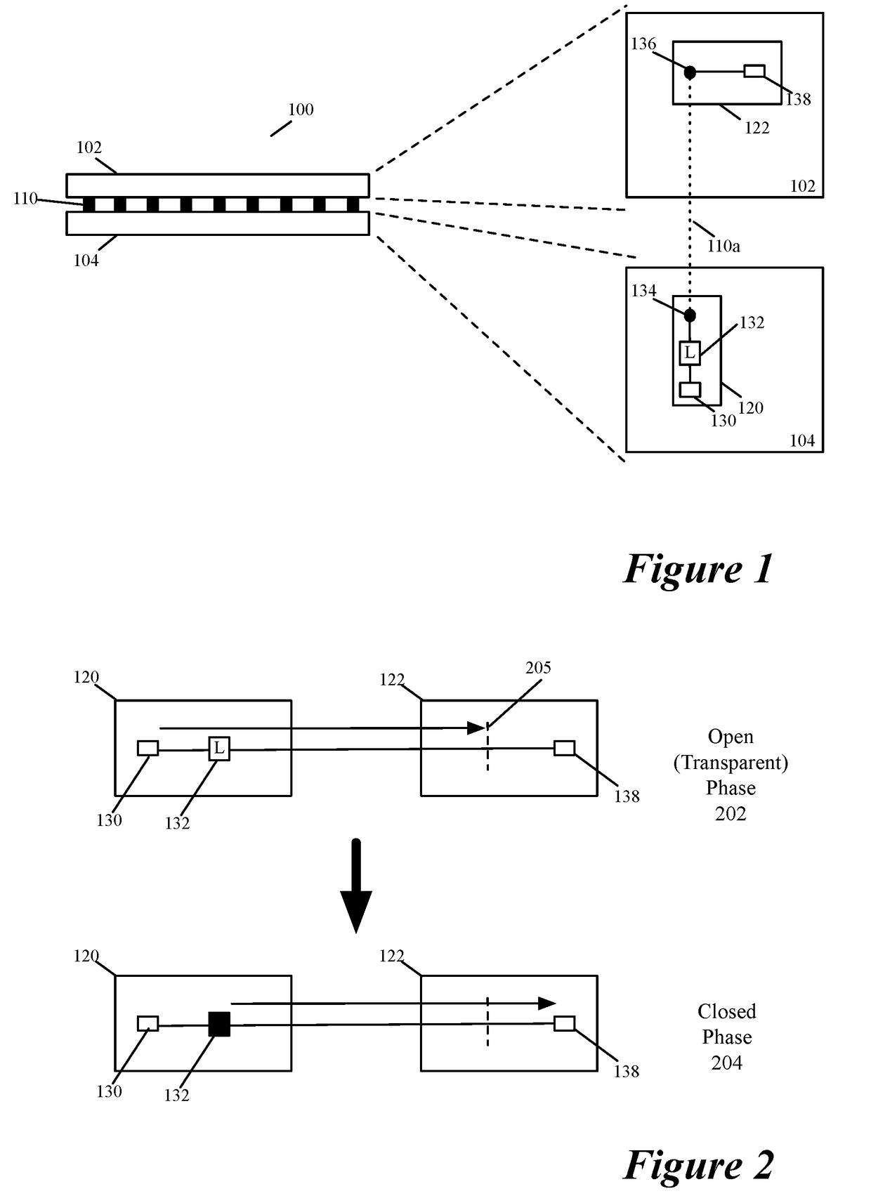
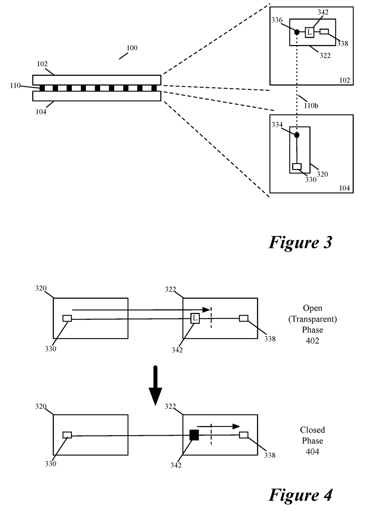
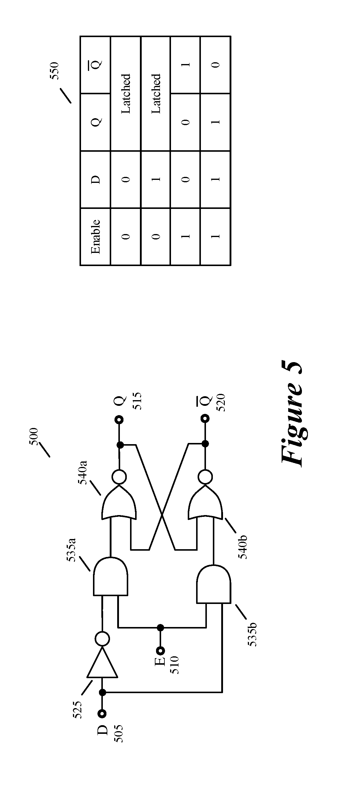
[0036]Some embodiments of the invention provide a three-dimensional (3D) circuit structure that uses latches to transfer signals between two bonded circuit layers. In some embodiments, this structure includes a first circuit partition on a first bonded layer and a second circuit partition on a second bonded layer. It also includes at least one latch to transfer signals between the first circuit partition on the first bonded layer and the second circuit partition on the second bonded layer. In some embodiments, the latch operates in (1) an open first mode (also called a transparent mode) that allows a signal to...


PUM


Abstract

Some embodiments provide a three-dimensional (3D) circuit structure that has two or more vertically stacked bonded layers with a machine-trained network on at least one bonded layer. As described above, each bonded layer can be an IC die or an IC wafer in some embodiments with different embodiments encompassing different combinations of wafers and dies for the different bonded layers. The machine-trained network in some embodiments includes several stages of machine-trained processing nodes with routing fabric that supplies the outputs of earlier stage nodes to drive the inputs of later stage nodes. In some embodiments, the machine-trained network is a neural network and the processing nodes are neurons of the neural network. In some embodiments, one or more parameters associated with each processing node (e.g., each neuron) is defined through machine-trained processes that define the values of these parameters in order to allow the machine-trained network (e.g., neural network) to perform particular operations (e.g., face recognition, voice recognition, etc.). For example, in some embodiments, the machine-trained parameters are weight values that are used to aggregate (e.g., to sum) several output values of several earlier stage processing nodes to produce an input value for a later stage processing node.

Description

BACKGROUND[0001]In recent years, there have been great advances in the field of machine learning. Much of these advances have been in machine trained networks (e.g., deep neural networks) and algorithms for training such networks. However, there has not been as much advances in circuits for implementing machine-trained networks. This has been primarily due to an over reliance on implementing machine trained networks in datacenters as opposed to in devices in the real world. Therefore, there is a need in the art for innovative circuits for implementing machine trained networks as well as other types of designs.BRIEF SUMMARY[0002]Some embodiments of the invention provide a three-dimensional (3D) circuit structure that uses latches to transfer signals between two bonded circuit layers. In some embodiments, this structure includes a first circuit partition on a first bonded layer and a second circuit partition on a second bonded layer. It also includes at least one latch to transfer sig...

Claims


Application Information

Patent Timeline
IPC IPC(8): H01L25/065G06N3/04
CPCH01L25/0657G06N3/04H01L2225/06524H01L2225/06541H01L2225/06582H01L24/17H01L2224/16227H01L2224/17181H01L2924/16235G06N3/084G06N3/063H01L24/16H01L2224/16145H03K19/21G06F11/1423G06F11/2028G06F11/2041G06F11/2051H01L2225/06565H01L2225/06513G06N3/048G06N3/08H01L25/0756H01L25/043H01L2225/06503H01L25/117H01L25/074G06N3/065G06F11/2007G06F2201/85G06N3/082H01L23/3128H01L2224/16225H01L2225/06517H01L2225/06586
Inventor TEIG, STEVEN L.DUONG, KENNETHDELACRUZ, JAVIER
Owner XCELSIS CORP
Why Eureka
Try Eureka