Semiconductor package device and method of manufacturing the same
a technology of semiconductor devices and package devices, which is applied in the direction of semiconductor devices, semiconductor/solid-state device details, electrical apparatus, etc., can solve the problem that the relative wide opening of the nozzle may occupy a relatively large space in the packag
- Summary
- Abstract
- Description
- Claims
- Application Information
AI Technical Summary
Benefits of technology
Problems solved by technology
Method used
Image

Examples
Embodiment Construction
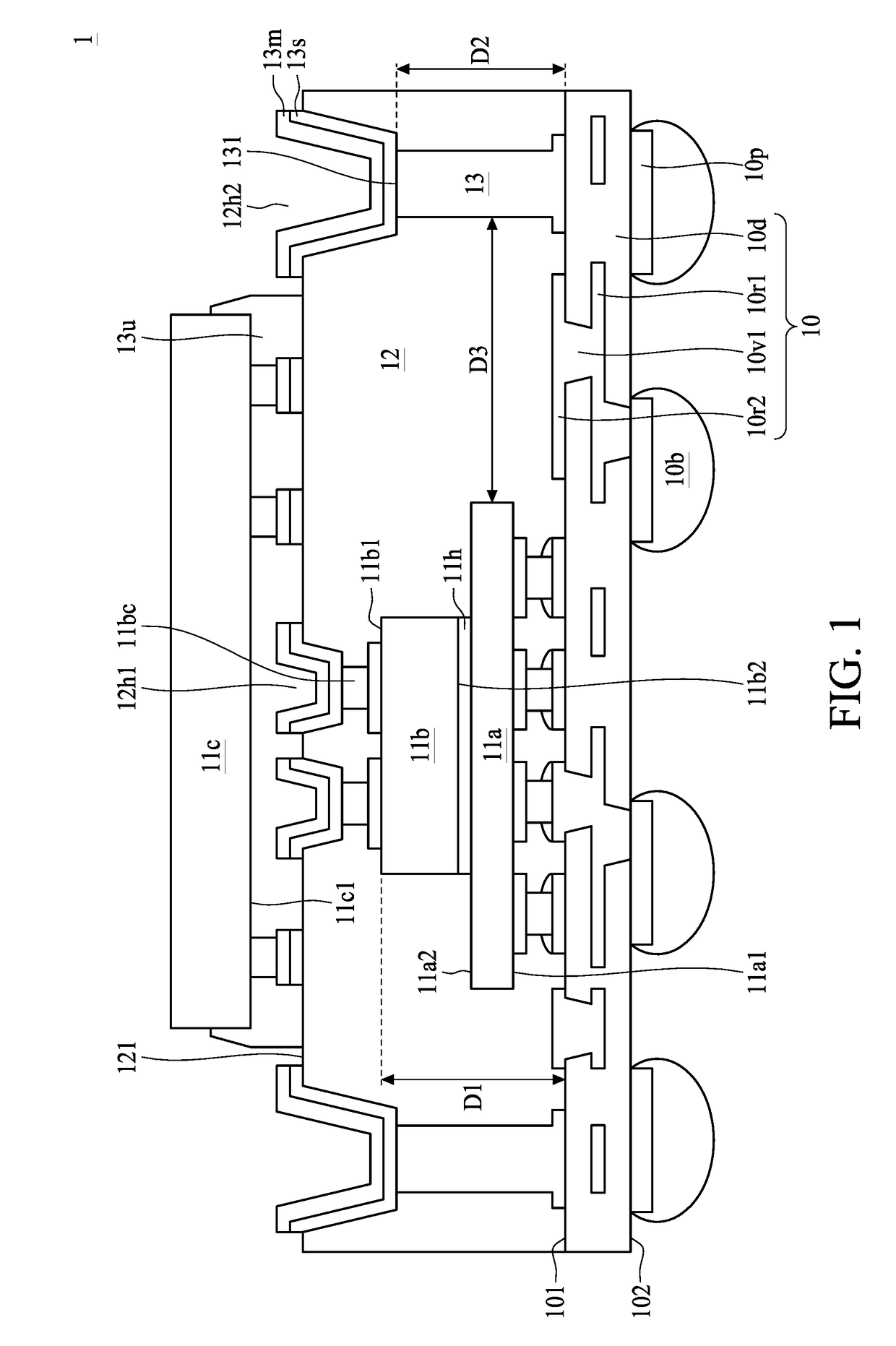
[0019]FIG. 1 illustrates a cross-sectional view of a semiconductor package device 1 in accordance with some embodiments of the present disclosure. The semiconductor package device 1 includes a circuit layer 10, electronic components 11a, 11b, 11c, a package body 12 and a conductive element 13.
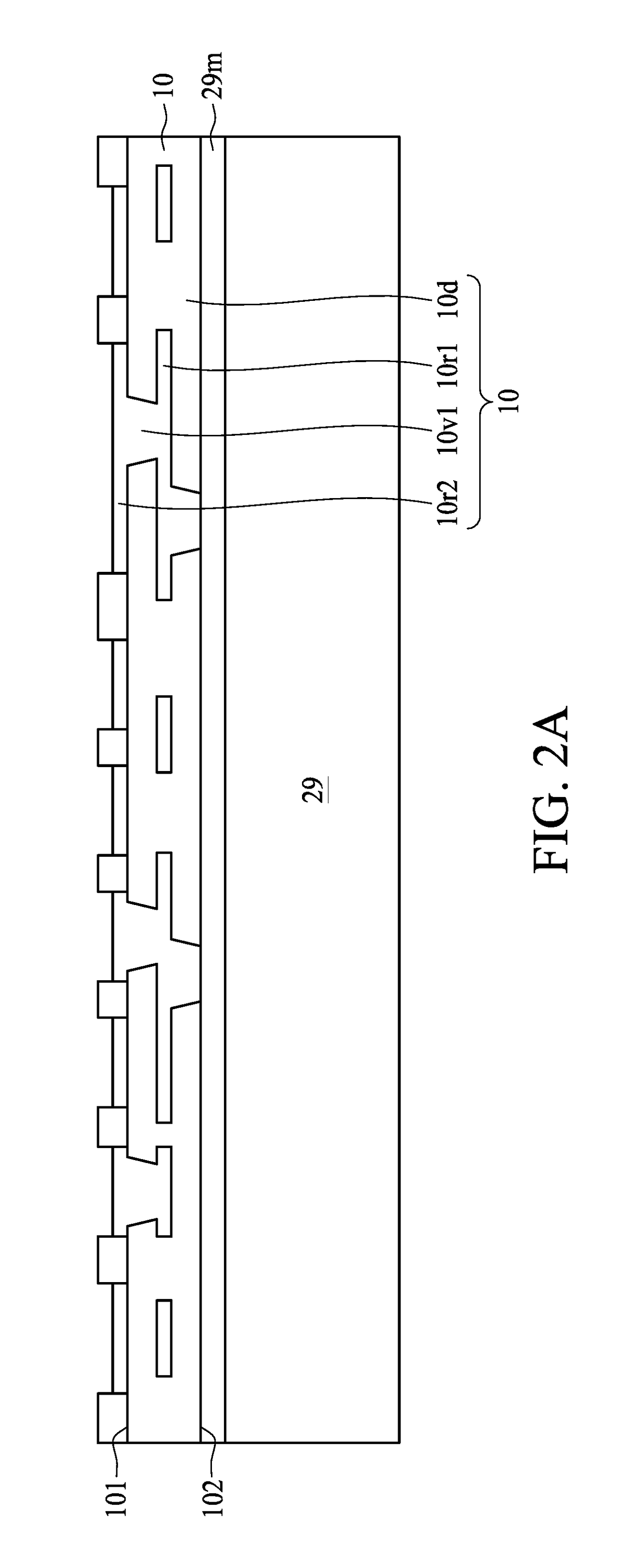
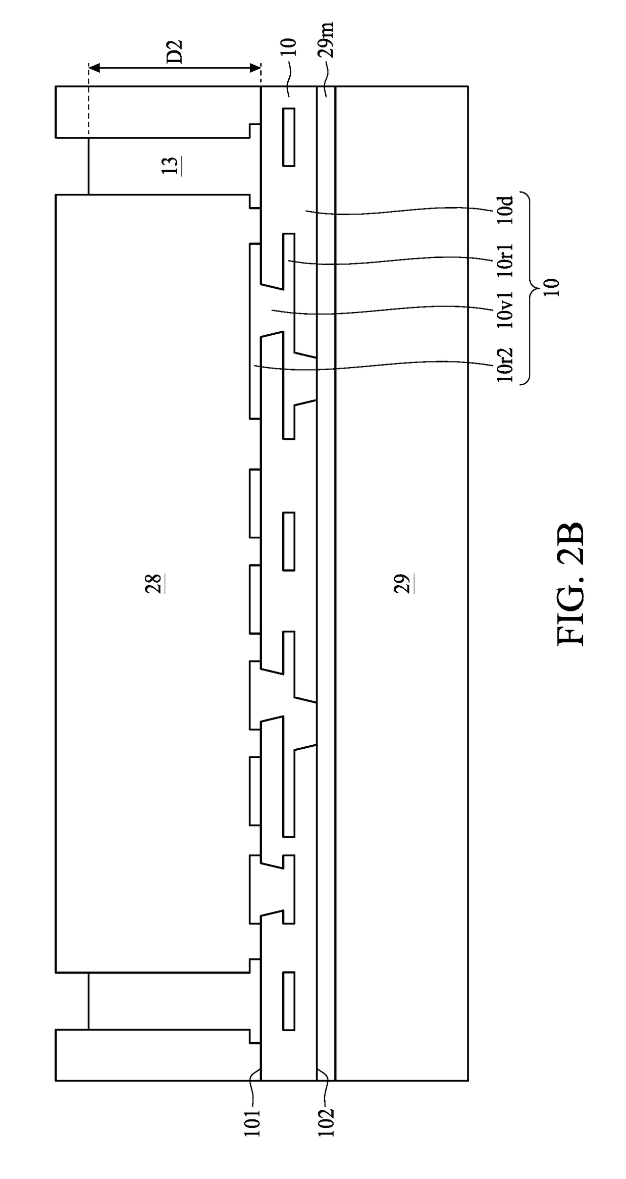
[0020]The circuit layer 10 includes a dielectric layer or an insulation layer 10d and conductive layers 10r1, 10r2 (which can include, for example, a metal layer) encapsulated or covered at least in part by the dielectric layer 10d. The conductive layers 10r1 and 10r2 are physically separated from each other and electrically connected through conductive interconnections 10v1 (e.g., vias). In some embodiments, the circuit layer 10 may include any number of dielectric layers and conductive layers. For example, the circuit layer 10 may include N dielectric layers and conductive layers, where N is an integer. In some embodiments, the dielectric layer 10d may include an organic component, a solder m...
PUM
 Abstract
Description
Claims
Application Information
 - R&D
- Intellectual Property
- Life Sciences
- Materials
- Tech Scout
- Unparalleled Data Quality
- Higher Quality Content
- 60% Fewer Hallucinations
Browse by: Latest US Patents, China's latest patents, Technical Efficacy Thesaurus, Application Domain, Technology Topic, Popular Technical Reports.
© 2025 PatSnap. All rights reserved.Legal|Privacy policy|Modern Slavery Act Transparency Statement|Sitemap|About US| Contact US: help@patsnap.com