Semiconductor device and fabrication method thereof

a technology of semiconductor devices and semiconductors, applied in the field of semiconductor devices of silicon-oscillating devices, can solve problems such as the apparent charge effect, and achieve the effect of improving deficiencies and disadvantages

Inactive Publication Date: 2019-02-14
UNITED MICROELECTRONICS CORP
View PDF4 Cites 3 Cited by
  • Summary
  • Abstract
  • Description
  • Claims
  • Application Information

AI Technical Summary

Benefits of technology

[0005]It is one object of the present invention to provide a semiconductor device and a method of making the same, which can improve the deficiencies and disadvantages of the prior art.

Problems solved by technology

The disadvantage of this practice is that the conductive contact structure with the insulating liner leads to apparent induced charge effect.

Method used


Image

  • Semiconductor device and fabrication method thereof
  • Semiconductor device and fabrication method thereof
  • Semiconductor device and fabrication method thereof

Examples


Embodiment Construction

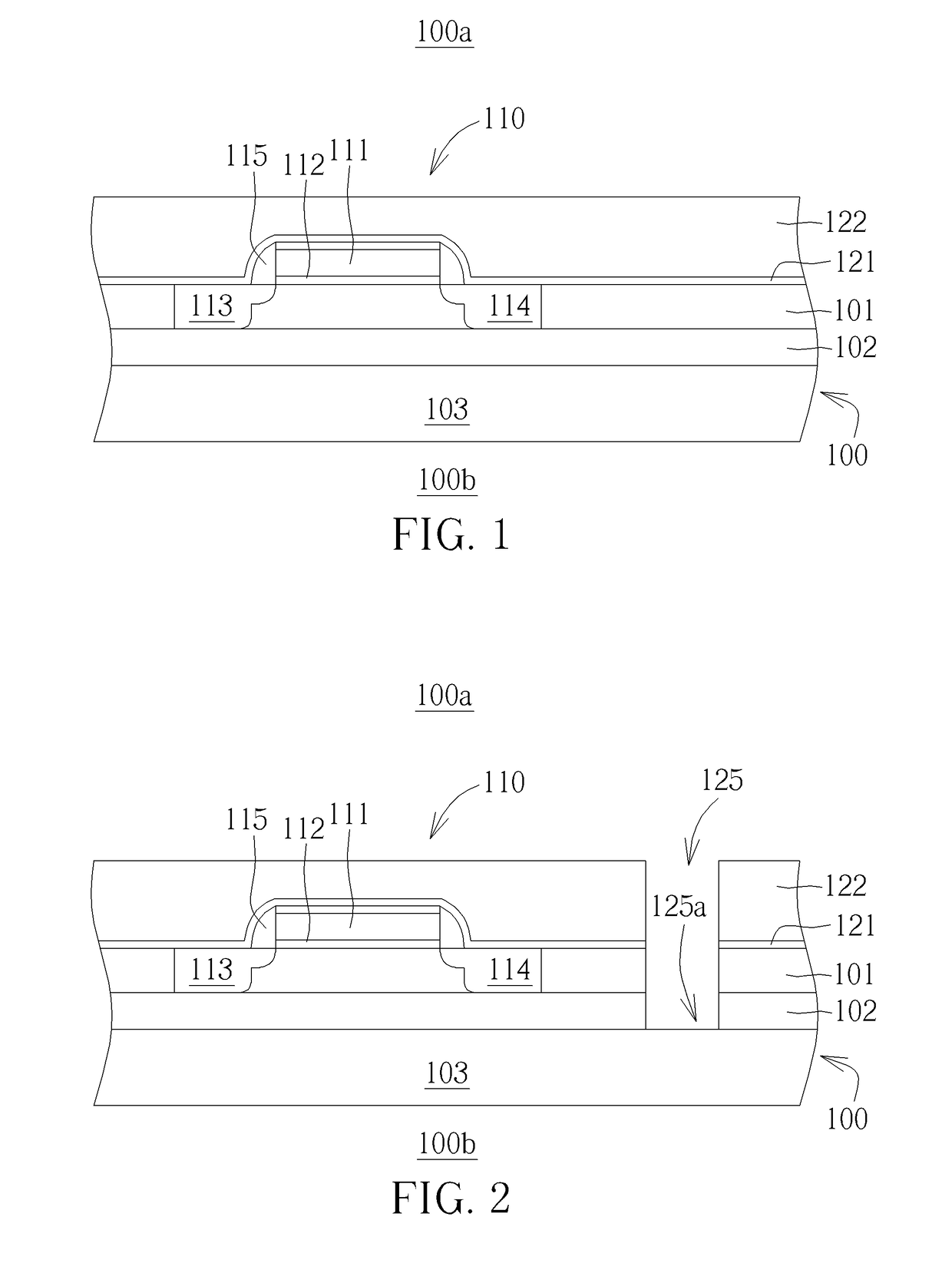
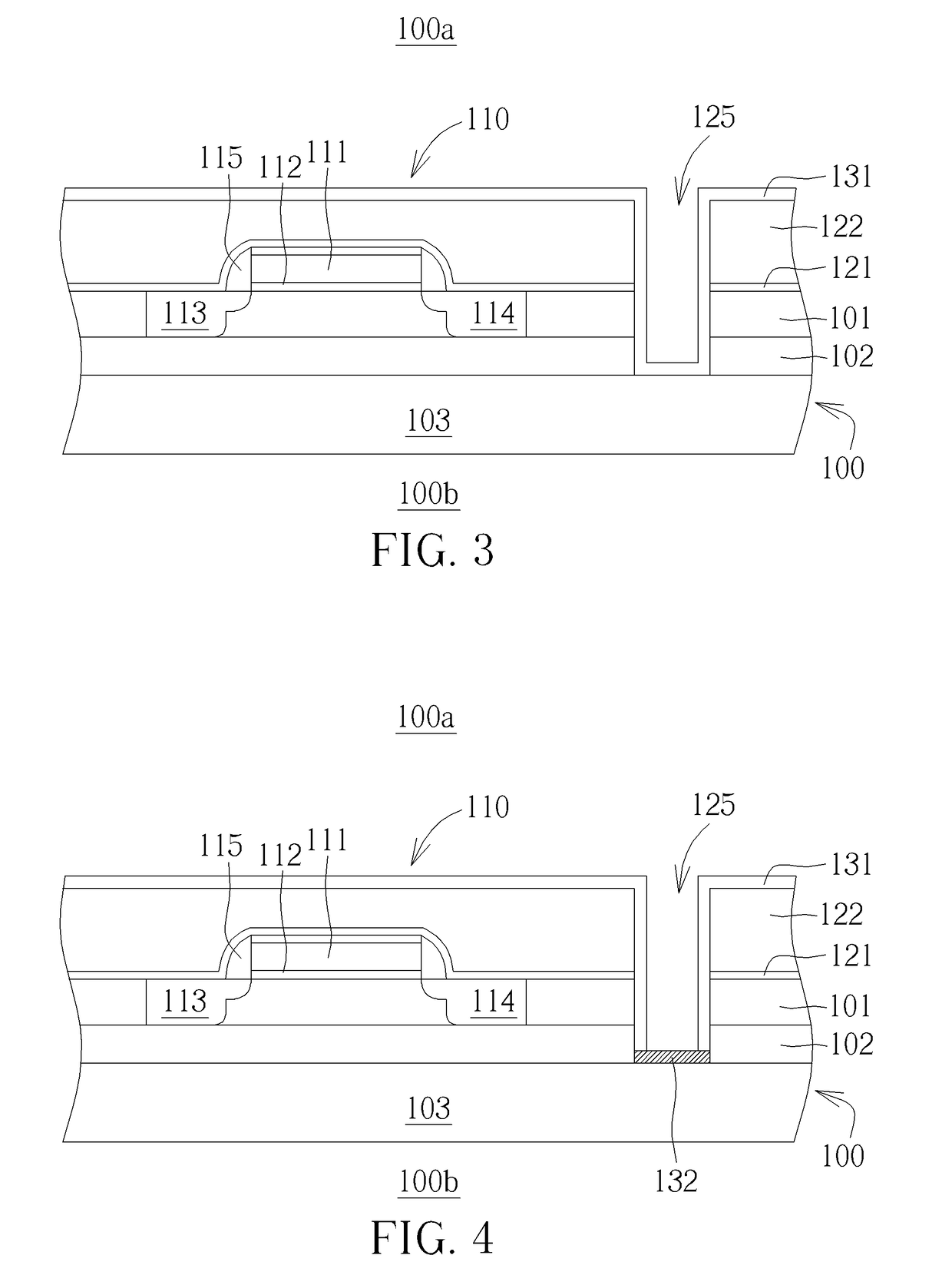
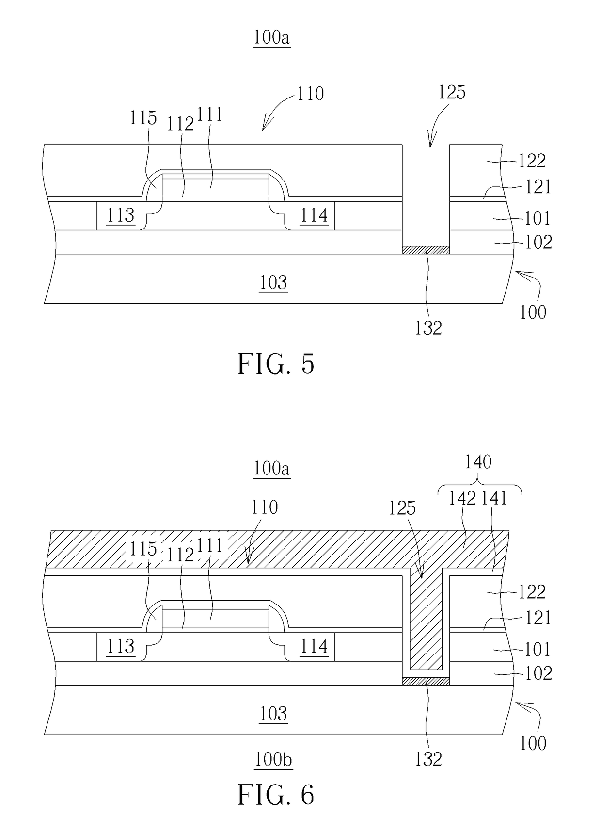
[0016]In the following detailed description of the disclosure, reference is made to the accompanying drawings, which form a part hereof, and in which is shown, by way of illustration, specific embodiments in which the invention may be practiced. These embodiments are described in sufficient detail to enable those skilled in the art to practice the invention. Other embodiments may be utilized and structural changes may be made without departing from the scope of the present disclosure.

[0017]The following detailed description is, therefore, not to be taken in a limiting sense, and the scope of the present invention is defined only by the appended claims, along with the full scope of equivalents to which such claims are entitled. One or more implementations of the present invention will now be described with reference to the attached drawings, wherein like reference numerals are used to refer to like elements throughout, and wherein the illustrated structures are not necessarily drawn ...


PUM


Abstract

A semiconductor device includes a substrate having a frontside and a backside. The substrate includes a semiconductor layer and a buried insulator layer. A transistor is disposed on the semiconductor layer. An interlayer dielectric (ILD) layer is disposed on the frontside and covering the transistor. A contact structure penetrates through the ILD layer, the semiconductor layer and the buried insulator layer. A silicide layer caps an end surface of the contact structure on the backside. A passive element is disposed on the backside of the substrate. The contact structure is electrically connected to the passive element.

Description

CROSS REFERENCE TO RELATED APPLICATION[0001]This application claims the priority from CN application No. 201710690789.1, filed Aug. 14, 2017, which is included in its entirety herein by reference.BACKGROUND OF THE INVENTION1. Field of the Invention[0002]The present invention relates to the field of semiconductor technology, and in particular to a silicon-on-insulator (SOI) semiconductor device and a fabrication method thereof.2. Description of the Prior Art[0003]Devices fabricated using semiconductor-on-insulator (SOI) technologies may exhibit certain performance improvements in comparison with comparable devices built directly in a bulk silicon substrate. Generally, an SOI wafer includes a thin device layer of semiconductor material, a handle substrate, and a thin buried insulator layer, such as a buried oxide or BOX layer, physically separating and electrically isolating the device layer from the handle substrate. Integrated circuits are fabricated using the semiconductor material...

Claims


Application Information

Patent Timeline
Patent Type & Authority Applications(United States)
IPC IPC(8): H01L27/12H01L23/48H01L21/84H01L21/768H01L21/683
CPCH01L27/1203H01L27/13H01L21/76877H01L21/6835H01L21/76846H01L21/76898H01L2221/68327H01L2221/68359H01L24/05H01L24/03H01L2924/1205H01L2924/1206H01L2924/1207H01L2924/13091H01L23/53209H01L2224/05025H01L23/528H01L23/5226H01L21/32053H01L21/76889H01L21/76883H01L21/7624H01L21/02013H01L21/76879H01L21/76897H01L23/481H01L21/84H01L2221/6834
Inventor LI, WEN-SHENZHI, XIAOYUANCHEN, XINGXINGWEN, CHING-YANG
Owner UNITED MICROELECTRONICS CORP
Why Eureka
Try Eureka