MEMS probe and test device using the same

Active Publication Date: 2019-02-28
LEENO INDAL
View PDF1 Cites 2 Cited by
  • Summary
  • Abstract
  • Description
  • Claims
  • Application Information

AI Technical Summary

Benefits of technology

[0008]An aspect of the present disclosure is conceived to solve the conventional problems and provide an MEMS probe and a test dev

Problems solved by technology
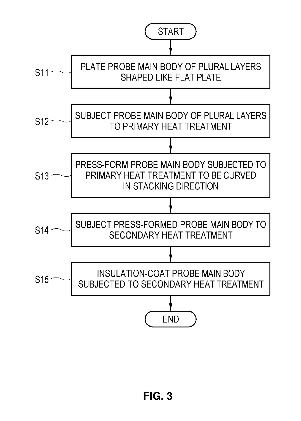
The cantilever type has disadvantages that all processes are modified and performed one by one by a human, but requires less production costs than the MEMS or vertical type.
However, it is complicated because a human has to arrange pins again one by one under a situation that needs repair or maintenance.
The MEMS or vertical type couples the MEMS probes by means of a precision instrument, which increases production costs but considerably improves precisi

Method used


Image

  • MEMS probe and test device using the same
  • MEMS probe and test device using the same
  • MEMS probe and test device using the same

Examples


first embodiment

[0035]FIG. 4 is a cross-sectional view of a test device 1 using the MEMS probe 100 according to the present disclosure.

[0036]The test device 1 includes a first support member 30 having a plurality of terminal holes 32, a second support member 40 having a plurality of guide holes 42 and spaced apart in parallel from the first support member 30, and a plurality of MEMS probes 100 of which opposite ends are inserted in the terminal holes 32 and the guide hole 42.

[0037]The first support member 30 is provided as an insulating plate member and has the plurality of terminal holes 32 in which the terminal contact portions 110 of the MEMS probes 100 are inserted.

[0038]The second support member 40 is provided as an insulating plate member and has the plurality of guide holes 42 in which the sliding contact portions 130 are inserted while sliding to move close to and away from the terminal contact portion 110.

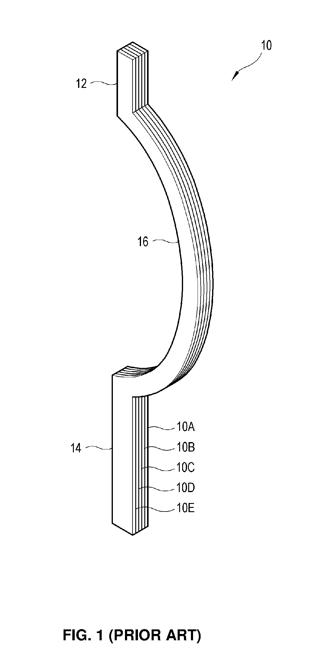
[0039]The MEMS probe 100 is the same as that shown in FIG. 1, and thus repetitive des...

second embodiment

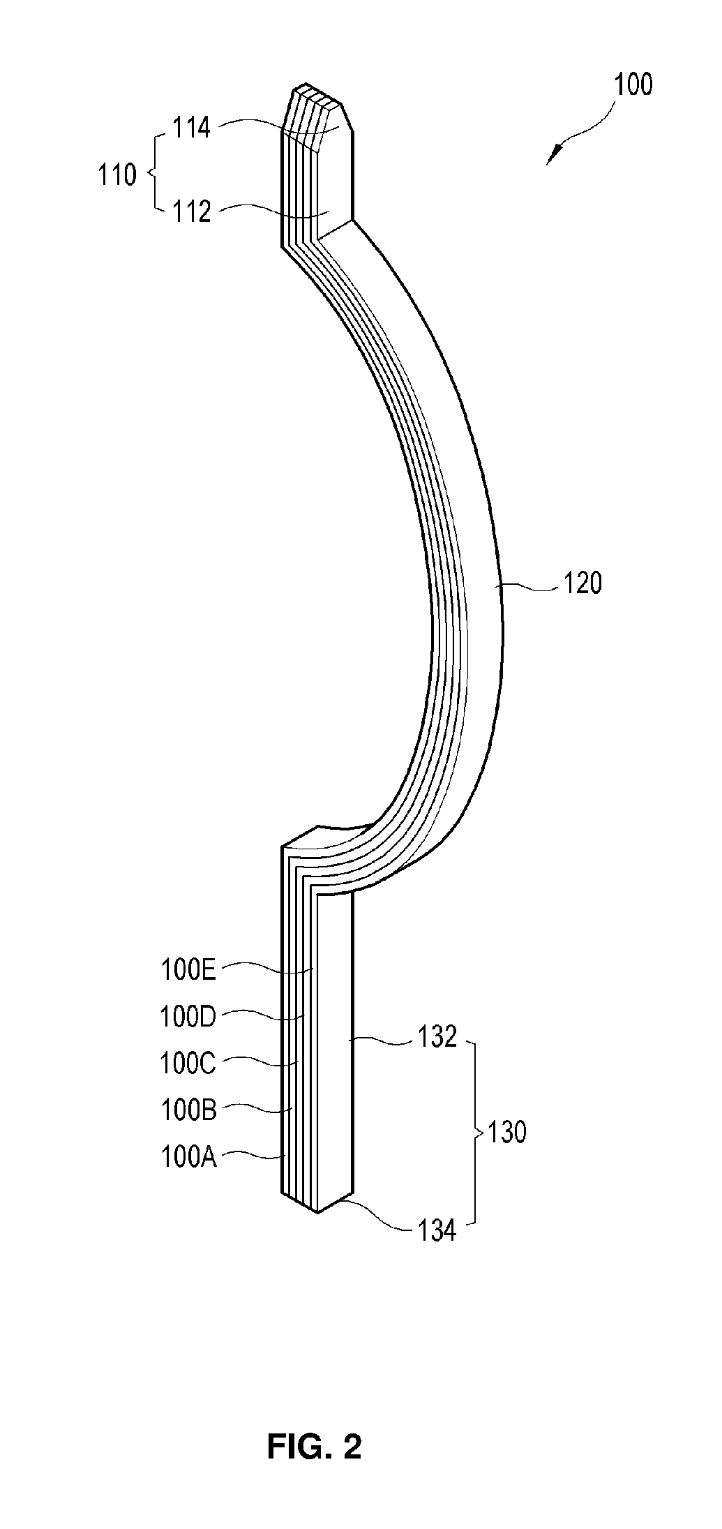
[0041]FIG. 5 is a perspective view of an MEMS probe 200 according to the present disclosure. As shown therein, the MEMS probe 200 includes five plating layers 200A, 200B, 200C, 200D and 200E and an insulation coating layer 200F covering an outer side of the plating layers, but is not limited thereto. The five plating layers 200A, 200B, 200C, 200D and 200E are stacked in a thickness direction, i.e. along a curved plane including a curved path of an elastic deformation portion. In other words, the five plating layers 200A, 200B, 200C, 200D and 200E are stacked in an elastic deformation direction of the elastic deformation portion 220. The insulation coating layer 200F prevents a short-circuit between a plurality of adjacent MEMS probes 200 applied to the test device 1, and prevents the plurality of stacked plating layers from being damaged or oxidized at a lateral side, thereby improving the durability of the MEMS probe 200. The insulation coating layer 200F may be selectively coated ...


PUM


Abstract

A microelectromechanical system (MEMS) probe for electric connection between a tested contact point of an object to be tested and a testing contact point of a test circuit. The MEMS probe includes: a first terminal contact portion; a second terminal contact portion movable close to and away from the first terminal contact portion; and an elastic connecting portion connecting the first terminal contact portion and the second terminal contact portion, elastically deformed by an approach of the second terminal contact portion and comprising a plurality of plating layers stacked in the elastic deformation direction. According to the present disclosure, the MEMS probe includes a plurality of plating layers stacked in the elastic deformation direction, thereby decreasing fatigue failure and improving durability.

Description

REFERENCE TO RELATED APPLICATIONS[0001]This application claims the priority benefit of Korean Patent Application No. 10-2017-0106770 filed on Aug. 23, 2017, the entire contents of which are incorporated herein by reference.FIELD OF THE INVENTION[0002]The present disclosure relates to a microelectromechanical system (MEMS) probe and a test device using the same for testing electric characteristics of a semiconductor or the like object to be tested.BACKGROUND OF THE INVENTION[0003]As a test device for testing electric characteristics or adequacy of a semiconductor wafer or the like object to be tested, a probe card has been used including a plurality of probes for electrical connection between a terminal of the object to be tested and a terminal of a test circuit board, and a probe supporter for supporting these probes.[0004]With development of technology, the semiconductor wafer has become larger and a semiconductor has become smaller. According as the number of semiconductor pads fo...

Claims


Application Information

Patent Timeline
IPC IPC(8): G01R1/067H01R13/03H01R13/24H01R43/16G01R1/073G01R31/28
CPCG01R1/06716H01R13/03H01R13/2471H01R43/16G01R1/07342G01R31/2886H01R2201/20G01R1/073H01R13/2407G01R1/07314G01R1/06761G01R1/07357G01R1/07307G01R3/00
Inventor PARK, UNG-GI
Owner LEENO INDAL
Why Eureka
Try Eureka