Piezoelectric element drive circuit

Active Publication Date: 2019-02-28
MURATA MFG CO LTD
View PDF0 Cites 0 Cited by
  • Summary
  • Abstract
  • Description
  • Claims
  • Application Information

AI Technical Summary

Benefits of technology

The present disclosure provides a piezoelectric element drive circuit that reduces wasteful power consumption and ripple in the drive current, which prevents the piezoelectric element from operating unnecessary. The circuit also includes an inductor that suppresses spike-like drive current, further reducing wasteful power consumption. These technical effects enhance the efficient operation of the piezoelectric element.

Problems solved by technology

On the other hand, the drive voltage having the rectangular wave contains a harmonic that does not contribute to substantial operation of the piezoelectric element and only consumes power.
Therefore, in this piezoelectric element drive circuit, power consumption cannot not be sufficiently reduced depending on factors other than the fact that the drive voltage is the rectangular wave.

Method used


Image

  • Piezoelectric element drive circuit
  • Piezoelectric element drive circuit
  • Piezoelectric element drive circuit

Examples


first embodiment

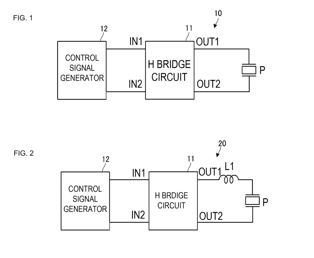
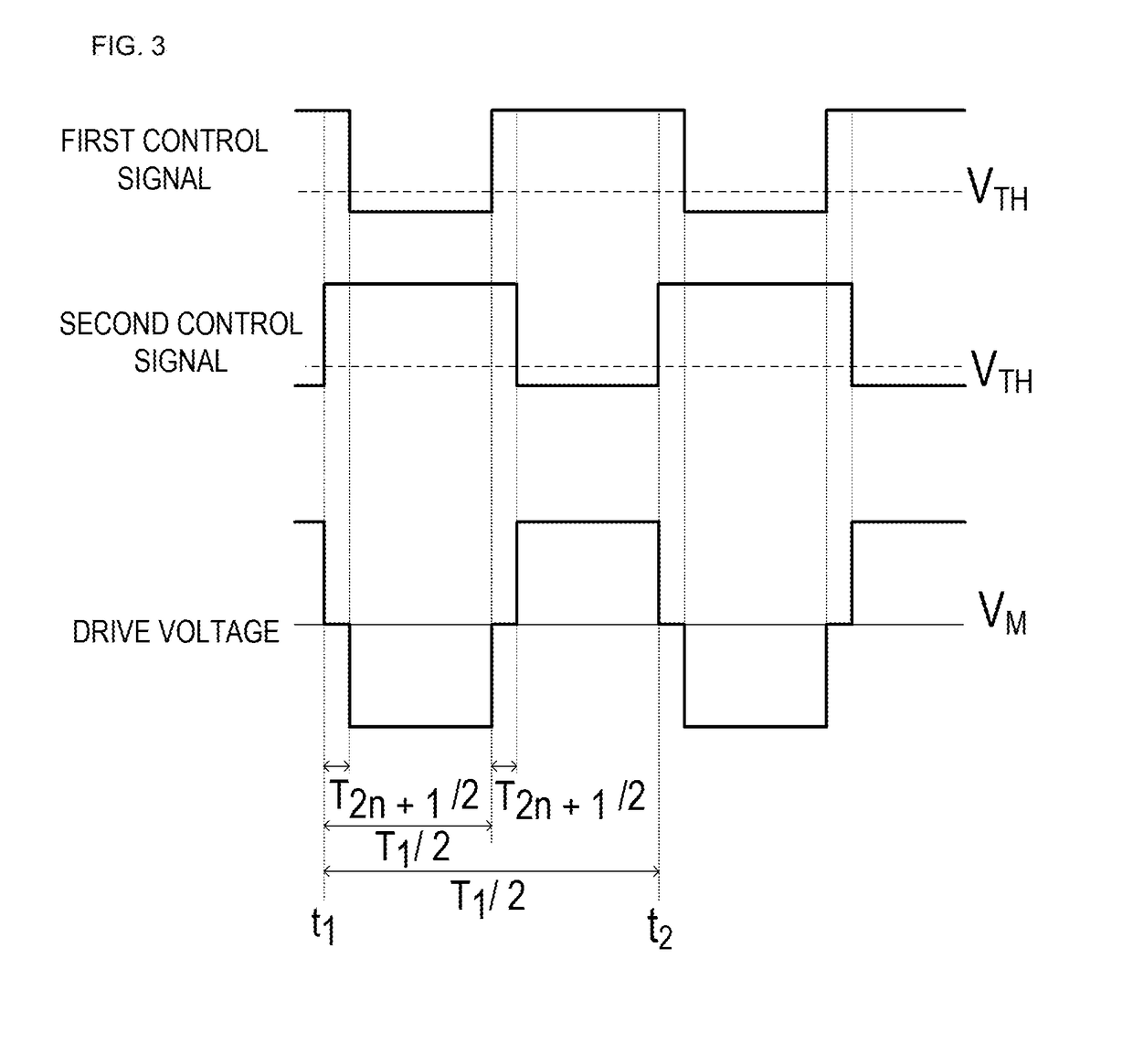
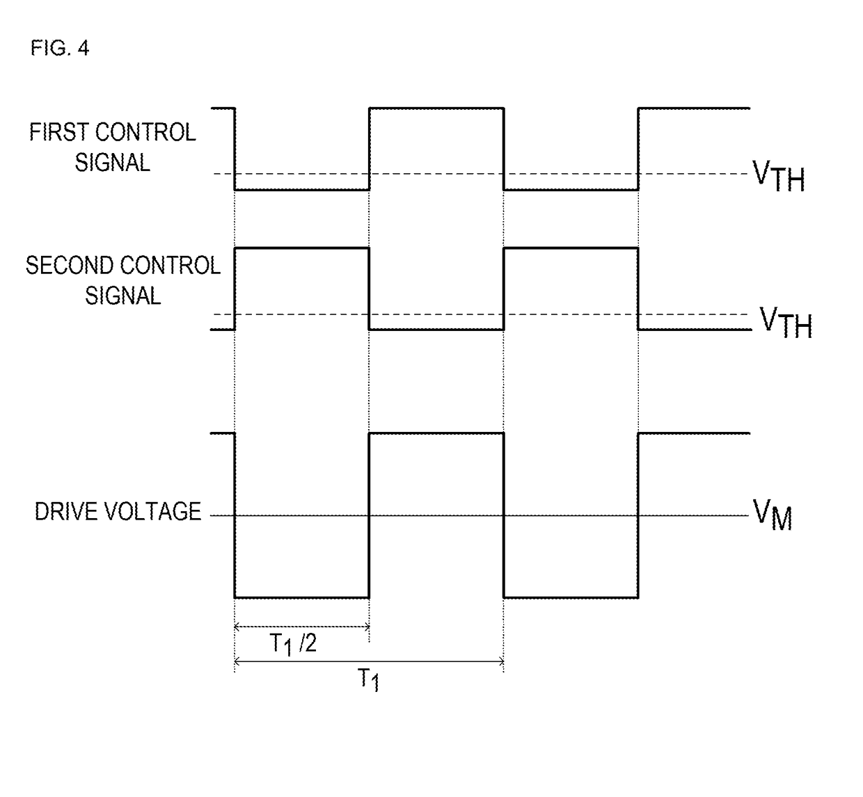
[0042]FIG. 1 is a block diagram of a piezoelectric element drive circuit 10 according to a first example of a first embodiment. The piezoelectric element drive circuit 10 includes an H bridge circuit 11 and a control signal generator 12. The H bridge circuit 11 is an example of a “drive voltage generator” of the disclosure. The H bridge circuit 11 has a first input terminal IN1, a second input terminal IN2, a first output terminal OUT1, and a second output terminal OUT2. The control signal generator 12 has a first control signal output terminal and a second control signal output terminal. The first input terminal IN1 of the H bridge circuit 11 is connected to the first control signal output terminal of the control signal generator 12. The second input terminal IN2 of the H bridge circuit 11 is connected to the second control signal output terminal of the control signal generator 12. The first output terminal OUT1 of the H bridge circuit 11 is connected to a first terminal of a piezo...

second embodiment

[0077]In a second embodiment, a period in which a drive voltage is a maximum value and a period in which the drive voltage is a minimum value are different from each other per cycle of the drive voltage. A first example of the second embodiment has a similar circuit configuration to that in the first example of the first embodiment (see FIG. 1). A second example of the second embodiment has a similar circuit configuration to that in the second example of the first embodiment (see FIG. 2).

[0078]FIG. 16 is a schematic diagram illustrating waveforms of drive voltages according to the first and second examples of the second embodiment. A cycle of the drive voltage is T1. The drive voltage is an intermediate potential for a period of time T2n+1 / 2, is a minimum value for a subsequent period of time TA−T2n−1 / 2, is the intermediate potential for a subsequent period of time T2n+1 / 2, and is a maximum value for a subsequent period of time T1−TA−T2n+1 / 2. The drive voltage periodically repeats t...

third embodiment

[0084]In a first example of a third embodiment, a period of time for which a drive voltage remains at an intermediate potential after the drive voltage falls to the intermediate potential and a period of time for which the drive voltage remains at the intermediate potential after the drive voltage rises to the intermediate potential are different from each other. FIG. 22 is a schematic diagram illustrating a waveform of the drive voltage according to the first example of the third embodiment. A cycle of the drive voltage is T1. The drive voltage is the intermediate potential for a period of time TB, is a minimum value for a subsequent period of time T1 / 2−TB, is the intermediate potential for a subsequent period of time T2n+1−TB, and is a maximum value for a subsequent period of time T1 / 2−(T2n+1−TB). The drive voltage periodically repeats this step-like transition. The period of time TB has a value which is different from time T2n+1 / 2.

[0085]In a second example of the third embodiment...


PUM


Abstract

A piezoelectric element drive circuit includes a piezoelectric element driven at a predetermined frequency and having a resonant frequency of (2n+1) times the predetermined frequency (n is a predetermined natural number), and a drive voltage generator that has a first output terminal connected to a first terminal of the piezoelectric element and a second output terminal connected to a second terminal of the piezoelectric element. When the piezoelectric element is driven, a waveform of potential difference between the first output terminal and the second output terminal is a step wave which transitions while taking an intermediate potential. A time length for which the potential difference is the intermediate potential is around (t2−t1) / (2n+1) in a period of time from time t1 at which the potential difference falls to the intermediate potential to time t2 at which the potential difference falls to the intermediate potential subsequently.

Description

[0001]This is a continuation of International Application No. PCT / JP2017 / 017236 filed on May 2, 2017 which claims priority from Japanese Patent Application No. 2016-094964 filed on May 11, 2016. The contents of these applications are incorporated herein by reference in their entireties.BACKGROUND OF THE DISCLOSUREField of the Disclosure[0002]The present disclosure relates to a piezoelectric element drive circuit that drives a piezoelectric element.Description of the Related Art[0003]An existing piezoelectric element drive circuit is disclosed in, for example, Patent Document 1. The piezoelectric element drive circuit includes an H bridge circuit, a resistor, a differential amplifier circuit, an inverting circuit, a first comparator, and a second comparator. The H bridge circuit has a first input terminal and a second input terminal, and a first output terminal and a second output terminal that are respectively connected to both terminals of a piezoelectric element. The resistor is c...

Claims


Application Information

Patent Timeline
IPC IPC(8): H01L41/113H01L41/04H02N2/06F04B17/00
CPCH02N2/06F04B17/003H01L41/113H01L41/042F04B43/046F04B49/06F04B49/065H10N30/802H10N30/20H10N30/30
Inventor OKAGUTI, KENJIRO
Owner MURATA MFG CO LTD
Why Eureka
Try Eureka