Semiconductor circuit using positive feedback field effect transistor for emulating neuron firing process

a positive feedback field and transistor technology, applied in pulse generators, pulse techniques, instruments, etc., can solve the problems of large power consumption, high supply voltage, and relative high endurance of the device, so as to reduce the waste of power consumption, reduce power consumption, and achieve the effect of the same endurance level

Active Publication Date: 2019-12-31
SEOUL NAT UNIV R&DB FOUND
View PDF3 Cites 0 Cited by
  • Summary
  • Abstract
  • Description
  • Claims
  • Application Information

AI Technical Summary

Benefits of technology

[0008]The present invention is to provide semiconductor circuits for emulating a neuron firing process using a positive feedback transistor. In the present invention, the positive feedback transistor has two gates in series to perform a neuron firing process with low power and to minimize power consumption when the neuron circuit is fired or not.
[0015]The present invention comprises a positive feedback transistor having first and second gate electrodes in the longitudinal direction of a channel region, wherein the first gate electrode is connected to a gate electrode of a first p-channel MOSFET to be an input terminal and the second gate electrode is connected to a drain to be applied with a supply voltage. And the present invention can separately accumulate electrons and holes in a channel region (i.e., a body) under each of gate electrodes by applying input signals to the input terminal and drastically reduce the wasted power consumption in the non-fired neurons because of the current turned on and off only at a moment when it corresponds to a firing of the neuron. Thus, the present invention can be driven by low power and have the same level of endurance as a general MOSFET.

Problems solved by technology

However, when holes formed by impact ionization are stored in the floating body, a relatively high supply voltage is required and there are disadvantages in terms of endurance of the device.
At this time, even when the potential stored in Cmem is smaller than the switching voltage, the current continues to flow to the subsequent amplifier A. So it causes a problem that power consumption becomes very large when the neuron is not fired.

Method used


Image

  • Semiconductor circuit using positive feedback field effect transistor for emulating neuron firing process
  • Semiconductor circuit using positive feedback field effect transistor for emulating neuron firing process
  • Semiconductor circuit using positive feedback field effect transistor for emulating neuron firing process

Examples


Embodiment Construction

[0028]Detailed descriptions of preferred embodiments of the present invention are provided below with reference to accompanying drawings. The structures or the electrical characteristic diagrams of exemplified devices and circuits in the accompanying drawings are provided to explain the technical idea of the present invention in order to understand a person with ordinary skill in the art to which the present invention pertains, thus, the technical idea of the present invention should not be restricted to the described embodiments herein.

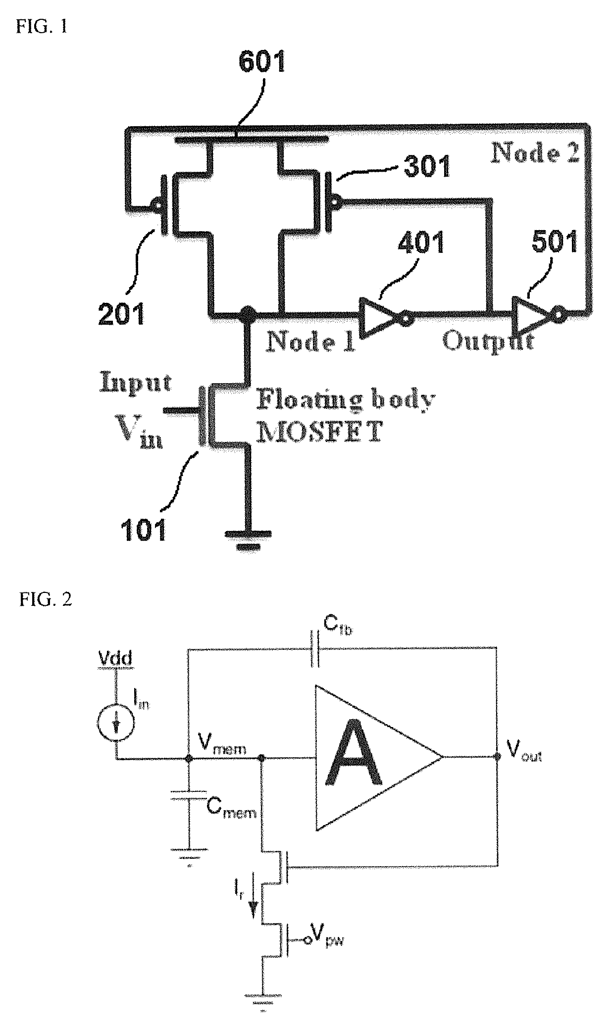
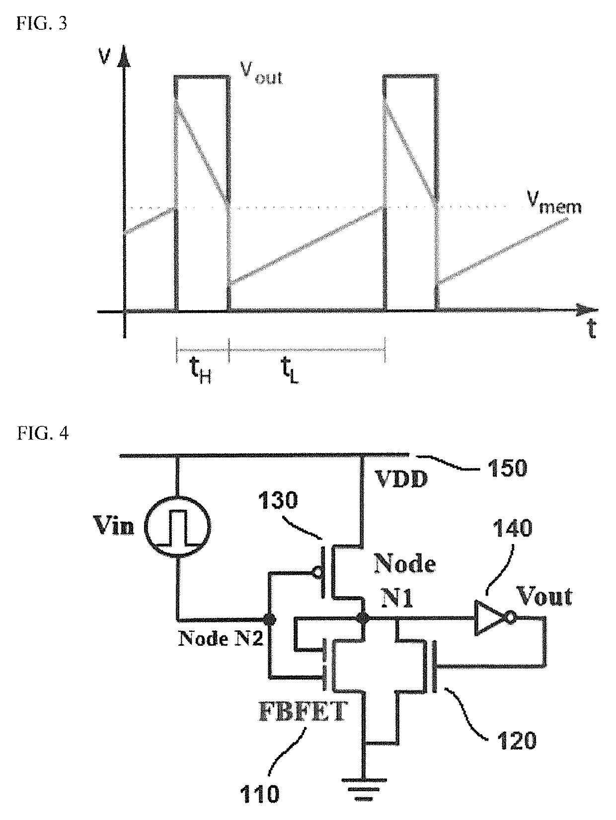
[0029]A semiconductor circuit for emulating a neuron firing process according to an embodiment of the present invention, as shown in FIG. 4, comprises: a positive feedback transistor 110 and a first n-channel MOSFET 120 connected in parallel between a ground GND and a first node Node N1; a first p-channel MOSFET 130 connected between the first node Node N1 and an electric power supply line 150; and an inverter 140 connected between the first node Nod...


PUM


Abstract

Semiconductor circuits are provided for emulating neuron firing process using a positive feedback transistor having first and second gate electrodes in the longitudinal direction of a channel region. The first gate electrode is connected to a gate electrode of a first p-channel MOSFET to be an input terminal and the second gate electrode is connected to a drain to be applied with a supply voltage. Thus electrons and holes can accumulate separately in a channel region (i.e., a body) under each of the gate electrodes by applying input signals to the input terminal and drastically reduce the wasted power consumption in the non-fired neurons because the current is turned on and off only at a moment that corresponds to a firing of the neuron. Thus, the semiconductor circuits can be driven by low power and have the same level of endurance as a general MOSFET.

Description

CROSS-REFERENCE TO RELATED APPLICATION[0001]This application claims priority to Korean Patent Application No. 10-2017-0079213, filed on Jun. 22, 2017, under 35 U.S.C. 119, the entire contents of which are hereby incorporated by reference.BACKGROUNDField of the Invention[0002]The present invention relates to semiconductor circuits, and more particularly to semiconductor circuits for emulating a neuron firing process using a positive feedback field effect transistor (FBFET).Description of the Related Art[0003]The nervous system of a living body is consisted of numerous nerve cell neurons and synapses connecting neurons. Thus, external stimulations are converted into electrical signals in the living body and the signals are transmitted into each nervous system in the form of action potentials through neurons. When the action potentials generated from pre-synaptic neurons pass through the synapses, they become small-sized post-synaptic potentials. When the various post-synaptic potentia...

Claims


Application Information

Patent Timeline
Patent Type & Authority Patents(United States)
IPC IPC(8): H03K17/687H01L29/10H01L29/08H01L29/739G06N3/10H01L29/423H03K3/012
CPCG06N3/10H01L29/7393H01L29/0847H03K17/6872H01L29/1033H01L29/4238H03K3/012G06N3/049H01L29/7391H01L29/423H01L29/10G06N3/065G06N3/063H03K19/08
Inventor PARK, BYUNG-GOOKKWON, MIN-WOOHWANG, SUNGMINBAEK, MYUNG-HYUNJANG, TAE-JIN
Owner SEOUL NAT UNIV R&DB FOUND
Why Eureka
Try Eureka