Fabrication of nano-structures on multiple sides of a non-planar surface

a nano-structure and non-planar surface technology, applied in the field of medical devices, can solve the problems of existing technologies methods were limited, existing technologies are not geared towards devices, etc., and achieve the effect of preventing the proliferation of microorganisms and increasing or reducing cell motility

Active Publication Date: 2019-03-14
RGT UNIV OF CALIFORNIA
View PDF0 Cites 5 Cited by
  • Summary
  • Abstract
  • Description
  • Claims
  • Application Information

AI Technical Summary

Benefits of technology

[0006]In various embodiments, disclosed herein is a method of transferring a microstructured or nanostructured polymer thin film to a curved surface, comprising: providing an elastomeric negative mold with microcavities or nanocavities, wherein the microcavities or nanocavities are the negative of the desired structures; spin-casting a polymer solution onto the elastomeric negative mold, which causes infiltration of the microcavities or nanocavities and creates a microstructured or nanostructured polymer thin film on the elastomer surface; and transferring the microstructured or nanostructured polymer thin film to the curved surface under heat and pressure. In one embodim...

Problems solved by technology

In another example, nano-structures were transferred on to a surface using soft lithography; however, this method was limited because it only applied to a limited range of elastomeric materials.
Existing technologies are not geared towards devices where micro- or nano-structures are present on multiple sides of th...

Method used


Image

  • Fabrication of nano-structures on multiple sides of a non-planar surface
  • Fabrication of nano-structures on multiple sides of a non-planar surface

Examples


example 1

Method of Making a Curved Patterned Surface

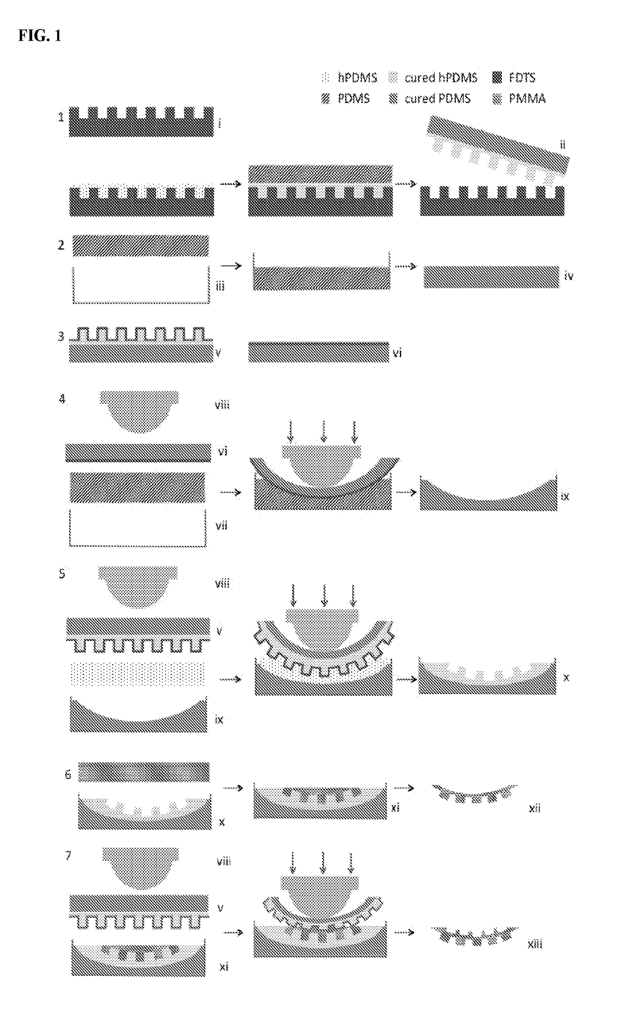
[0037]FIG. 1 illustrates one embodiment of the process of making a curved nano-structured polymer surface. In this embodiment, to make a curved patterned surface, the pattern is replicated onto a planar elastomer mold with soft lithography. Elastomers include silicone and polyurethane elastomers. A polymer precursor solution is applied into the curved elastomer mold. This results in a curved nanostructured polymer surface.

[0038]Referring to FIG. 1, in step 1, a hard mold (i) with nano-pillars with 300 nm periodicity was provided. The pillars were 190 nm in diameter and 300 nm in height. High modulus polydimethyl siloxane (hPDMS) was pipetted onto (i) and left at room temperature for 1.5 hours then cured at 65° C. for 0.5 hour. After the hPDMS was cured, polydimethyl siloxane (PDMS) prepolymer was poured on top and cured at 80° C. for one hour. After PDMS was cured, the planar silicone mold (ii) was demolded.

[0039]In step 2 of FIG. 1, PDMS w...

example 2

Curved PMMA Lens

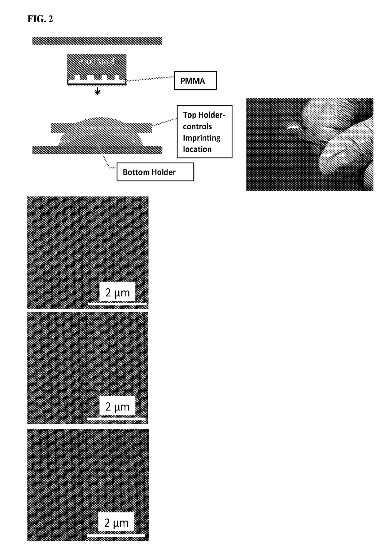
[0043]FIG. 2 illustrates one embodiment of the disclosure, describing a schematic of the process for making a curved poly-methylmethacralyte (PMMA) lens with nanostructures. In this embodiment, the inventors created a method for transferring a nanostructured polymer thin film to a curved polymer surface.

[0044]An elastomeric mold with the nano sized cavities, the negative of the desired structures, was fabricated (P300 Mold). Then the polymer solution was spin-cast onto the elastomeric negative mold such that it infiltrates the nano sized cavities and creates a residual layer on the elastomer surface. In this example, 5% (by weight) PMMA in toluene was used as the polymer solution. Finally, a curved piece of the same polymer was placed inside a holder and under heat and pressure. This process conformed the elastomer mold to the curved polymer piece. In some embodiments, if the temperature is at or above the glass transition temperature of the polymer, wetting might oc...


PUM

PropertyMeasurementUnit
Pressureaaaaaaaaaa
Microstructureaaaaaaaaaa

Abstract

In various embodiments, disclosed herein is a device comprising a non-planar surface, wherein nanostructures are fabricated on the non-planar surface. Also provided herein are methods of making and using a device comprising a non-planar surface, wherein nanostructures are fabricated on the non-planar surface. Further provided herein are methods of using a device comprising one or more non-planar surfaces, wherein the non-planar surfaces comprise one or more microstructures or nanostructures, comprising the steps: (a) using the device for its ordinary purpose; and (b) wherein the microstructures or nanostructures present in the device prevent proliferation of bacteria.

Description

FIELD OF THE INVENTION[0001]The present disclosure is in the medical and biomedical field, specifically medical devices.BACKGROUND OF THE DISCLOSURE[0002]Current literature provides some examples of transferring micro- and nano-structures to planar and curved surfaces. In one example, nano-structures were made on a pre-stretched flat surface. However, when the stretch was released, the film returned to the initial, non-planar shape. In another example, nano-structures were transferred on to a surface using soft lithography; however, this method was limited because it only applied to a limited range of elastomeric materials.[0003]In each of these existing technologies, only one side of the device displayed the micro- or nano-structures. Existing technologies are not geared towards devices where micro- or nano-structures are present on multiple sides of the device. Moreover, existing technologies are not geared towards devices where the micro- or nano-structures cover all the exposed ...

Claims


Application Information

Patent Timeline
IPC IPC(8): A01N25/34B29C59/02
CPCA01N25/34B29C59/021B29C59/022B29C59/026B29C2059/023B82Y40/00
Inventor YEE, ALBERTWU, SUSAN CHRISTINEDICKSON, MARY NORALIANG, ELENA
Owner RGT UNIV OF CALIFORNIA
Why Eureka
Try Eureka