Printed circuit board and electronic device

a printed circuit board and electronic device technology, applied in the direction of cross-talk/noise/interference reduction, conduction heat transfer modification, semiconductor/solid-state device details, etc., can solve the problems of large malfunction caused in the peripheral circuit, and more likely to be radiated by the noise current on the periphery. , to achieve the effect of reducing the influence on the peripheral electronic device, reducing the propagation path of the noise current n

Active Publication Date: 2019-05-02
SEIKO EPSON CORP
View PDF23 Cites 2 Cited by
  • Summary
  • Abstract
  • Description
  • Claims
  • Application Information

AI Technical Summary

Benefits of technology

[0008]An advantage of some aspects of the invention is to provide a printed circuit board that is capable of preventing an electromagnetic wave from being radiated to an outside.
[0010]According to such a configuration, a noise current which is generated in the electronic element to be propagated to the heat radiation member is propagated to the printed wiring board from the end portion of the heat radiation member. Since the end portion is disposed closer to the printed wiring board than the connection portion with the electronic element in the heat radiation member, a distance between the end portion of the heat radiation member and the printed wiring board becomes short. Thereby, since it is possible to shorten a propagation path of the noise current which is propagated to the printed wiring board from the end portion of the heat radiation member, it is possible to easily propagate the noise current to the printed wiring board. Accordingly, it is possible to prevent the noise current from being radiated to an outside of the printed circuit board as an electromagnetic wave, and it is possible to reduce an influence on a peripheral electronic device.
[0012]According to such a configuration, it is possible to dispose the end portion as described above, in accordance with the shape of the end portion. Accordingly, it is possible to form the heat radiation member that achieves effects described above, without complicating the heat radiation member.
[0015]On the contrary, according to the configuration described above, it is possible to increase the facing area of the portion corresponding to the end portion in the printed wiring board facing the end portion, in comparison with a case where the tip is in the shape which is sharp toward the printed wiring board. Thereby, it is possible to strengthen a coupling between the end portion of the heat radiation member and the facing area of the printed wiring board, in the same manner as a capacitive coupling of a capacitor, and it is possible to increase the noise current which is propagated to the printed wiring board from the end portion. Accordingly, it is possible to prevent the electromagnetic wave from being radiated to the outside of the printed circuit board, and it is possible to reduce the influence on the peripheral electronic device.
[0018]According to such a configuration, it is possible to efficiently transfer heat which is generated in the electronic element to the heat radiation member by the heat transfer member. Accordingly, it is possible to enhance cooling efficiency of the electronic element.
[0020]According to such a configuration, it is possible to easily propagate the noise current which heads toward the printed wiring board from the end portion of the heat radiation member to the ground of the printed wiring board. That is, it is possible to further increase the noise current which is propagated to the printed wiring board from the end portion of the heat radiation member. Accordingly, it is possible to effectively prevent the electromagnetic wave from being radiated to the outside of the printed circuit board, and it is possible to further reduce the influence on the peripheral electronic device.

Problems solved by technology

In such a case, there is a possibility that a malfunction is caused in a peripheral circuit or an electronic device.
Particularly, in the printed circuit board disclosed in JP-A-9-17921, there is a problem that a noise current which is generated in the integrated circuit or the like is propagated to the heat radiation board, the heat radiation board serves as an antenna, the electromagnetic wave is widely radiated on a periphery thereof, and an influence on a peripheral electronic device becomes large.
However, in the printed circuit board disclosed in JP-A-9-17921, since the heat radiation board is in a mere flat board shape, there is a problem that the noise current is more likely to be radiated on the periphery as an electromagnetic wave from an end portion of the heat radiation board than to be propagated to the printed substrate side through the stud.

Method used


Image

  • Printed circuit board and electronic device
  • Printed circuit board and electronic device
  • Printed circuit board and electronic device

Examples


embodiment

Modification of Embodiment

[0063]The invention is not limited to the embodiment described above, and the invention includes a case of being modified or improved within the scope which is capable of achieving the advantage of some aspects of the invention.

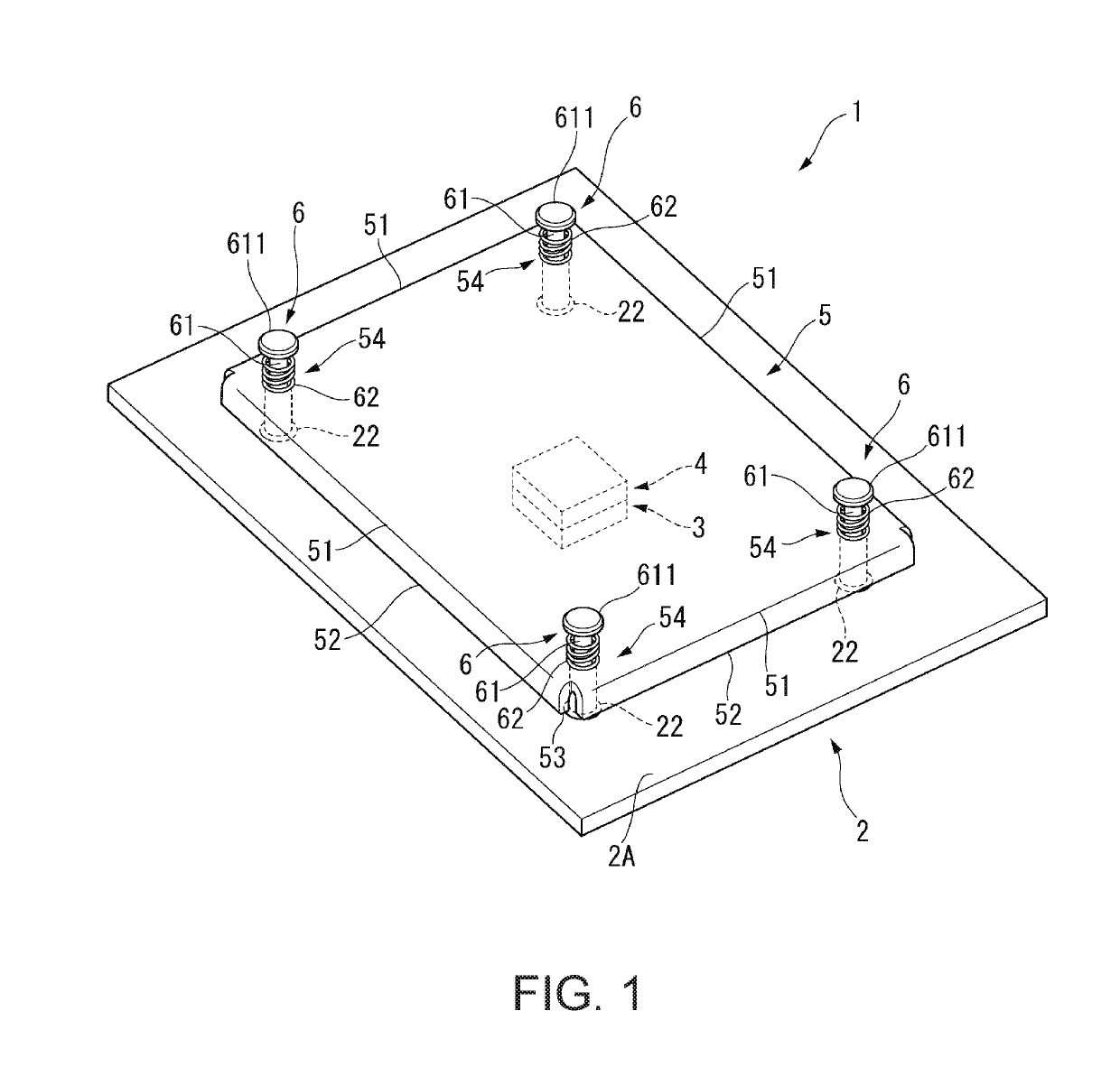
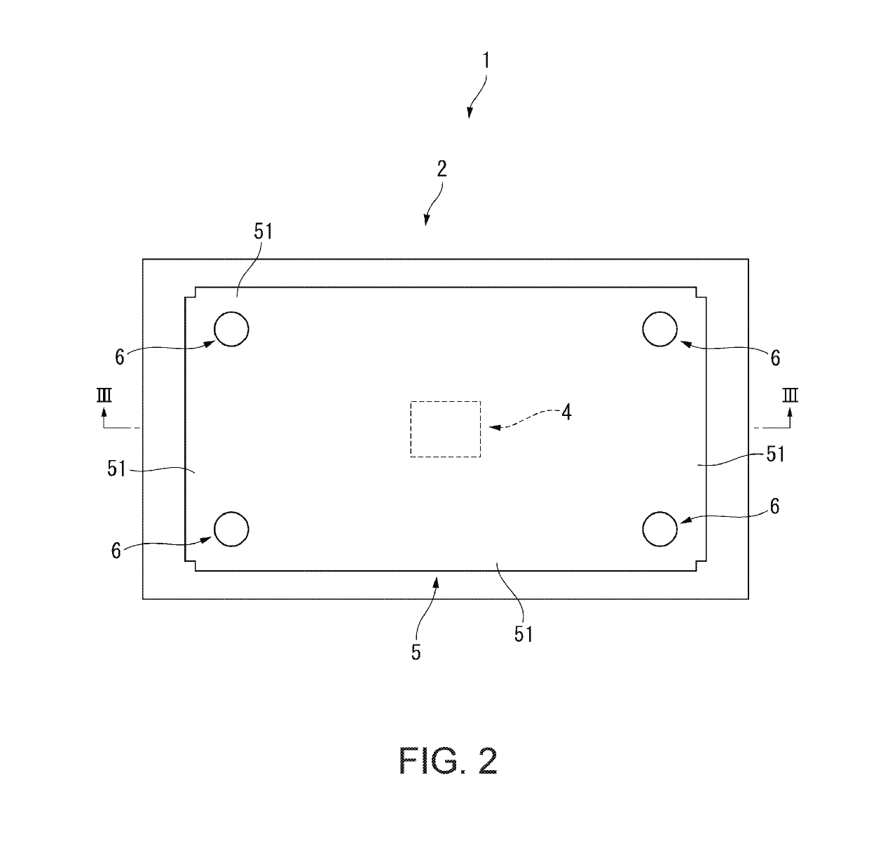
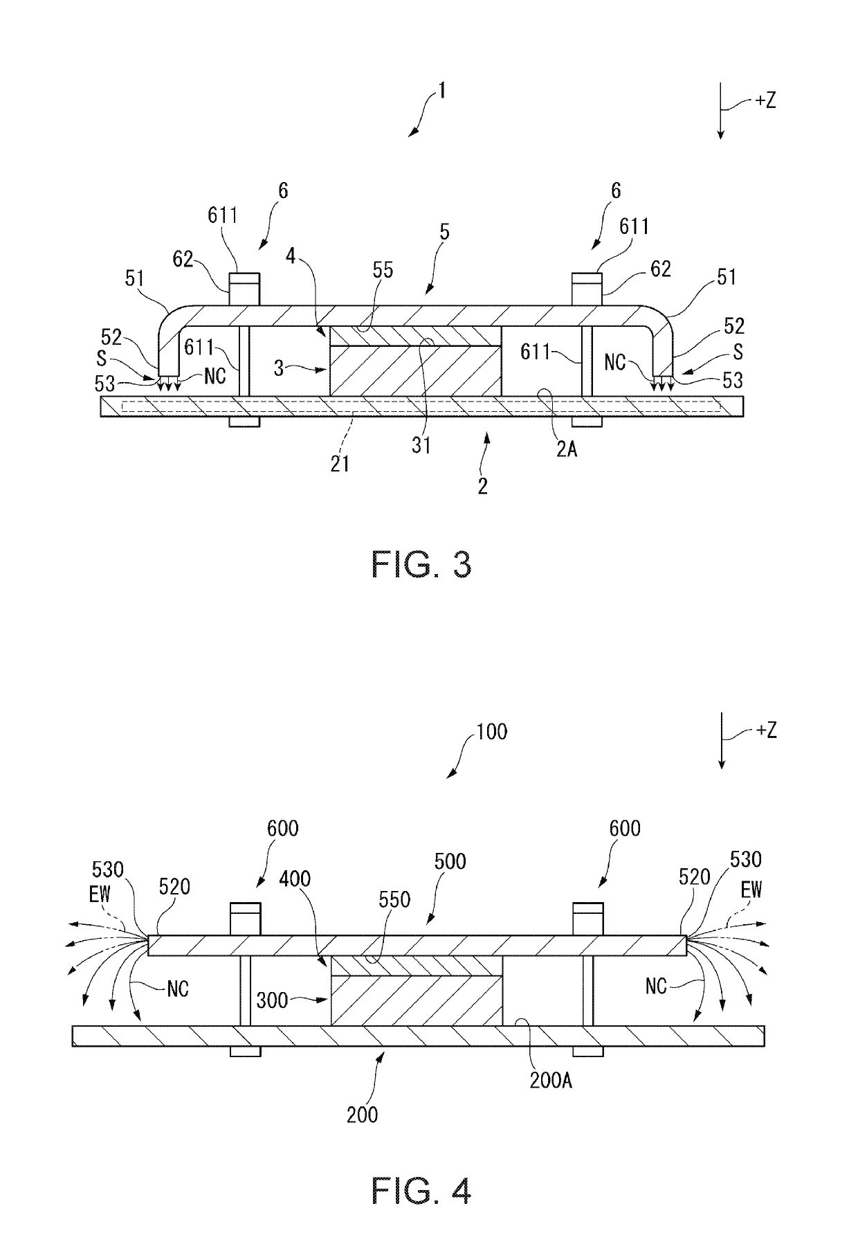
[0064]In the embodiment described above, the heat radiation board 5 has the bent deformation portion 51 which is bent to the printed wiring board 2, in the portion which reaches to the outer periphery of the heat radiation board 5 from the connection portion 55. However, the shape of the heat radiation board 5 is not limited thereto, and the shape thereof may be other shapes.

[0065]FIG. 5 is a sectional view illustrating a printed circuit board 1B as Modification Example 1 of the heat radiation board 5, and FIG. 6 is a sectional view illustrating a printed circuit board 1C as Modification Example 2.

[0066]For example, a heat radiation board 5B illustrated in FIG. 5, and a heat radiation board 5C illustrated in FIG. 6 are metal boards w...


PUM


Abstract

A printed circuit board includes a printed wiring board, an electronic element provided on a mounting surface of the printed wiring board, and a heat radiation member provided on an opposite side of a side on which the printed wiring board is positioned with respect to the electronic element, the heat radiation member thermally connected to the electronic element. An end portion of the heat radiation member is disposed closer to the printed wiring board than a connection portion with the electronic element in the heat radiation member, in a state where a space is provided between the end portion and the printed wiring board.

Description

BACKGROUND1. Technical Field[0001]The present invention relates to a printed circuit board and an electronic device.2. Related Art[0002]In the related art, there is known a printed circuit board including a printed wiring board, and a high heat-generating electronic element that is mounted on the printed wiring board. As such a printed circuit board, there is known a printed circuit board including a heat radiation board that radiates heat which is transferred from the electronic element (for example, see JP-A-9-17921).[0003]In the printed circuit board disclosed in JP-A-9-17921, a metal block is bonded to an upper portion of an integrated circuit with a thermally conductive adhesive, and a metal board as a heat radiation board is disposed in the metal block. In such a printed circuit board, the heat which is generated in the integrated circuit is transferred to the metal board through the metal block and the thermally conductive adhesive, and is radiated by the metal board, thereby...

Claims


Application Information

Patent Timeline
Patent Type & Authority Applications(United States)
IPC IPC(8): H05K1/02H05K7/20
CPCH05K1/0203H05K7/2039H01L23/3675H05K2201/066H01L23/4006H01L23/42H01L23/552H01L2023/4075H05K1/0216H05K2201/10409
Inventor SUEMATSU, NAOKI
Owner SEIKO EPSON CORP
Why Eureka
Try Eureka