S/n ratio improved photo-detection device and its manufacturing method

Inactive Publication Date: 2019-05-16
STANLEY ELECTRIC CO LTD
View PDF3 Cites 0 Cited by
  • Summary
  • Abstract
  • Description
  • Claims
  • Application Information

AI Technical Summary

Benefits of technology

The patent text is about a method for improving the signal-to-noise ratio (S / N ratio) of a photo-detection device. It explains that by making the area where light enters the device larger than the actual area of the photo semiconductor element, the amount of light that can be detected is increased, resulting in better S / N ratio. Additionally, the method does not require a metal mold, which reduces manufacturing costs.

Problems solved by technology

This would increase the manufacturing cost.

Method used


Image

  • S/n ratio improved photo-detection device and its manufacturing method
  • S/n ratio improved photo-detection device and its manufacturing method
  • S/n ratio improved photo-detection device and its manufacturing method

Examples


first embodiment

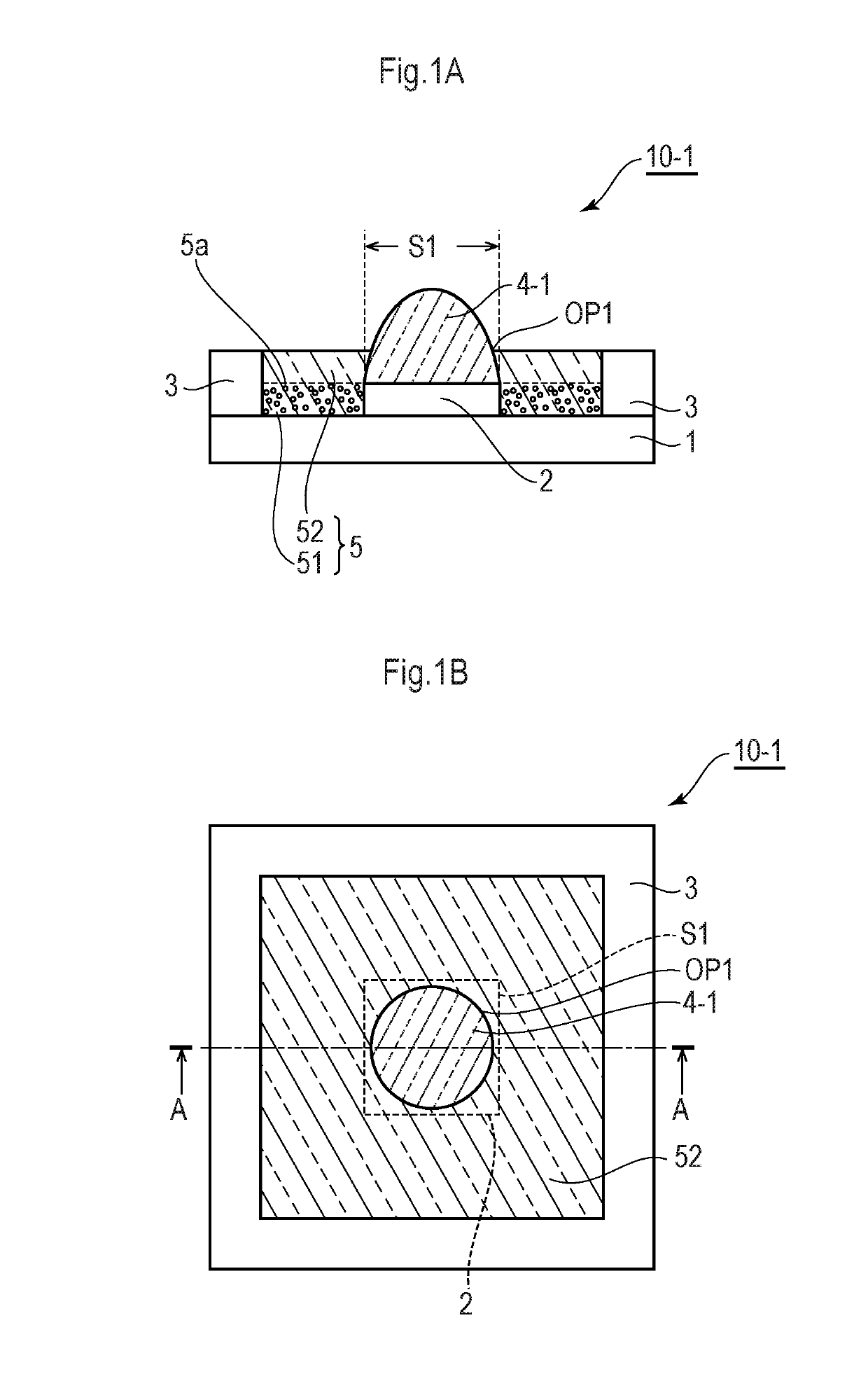
[0032]FIG. 1A is a cross-sectional view illustrating the photo-detection device according to the presently disclosed invention, and FIG. 1B is a plan view of the photo-detection device of FIG. 1A. Note that FIG. 1A is a cross-sectional view taken along the line A-A of FIG. 1B.

[0033]In FIGS. 1A and 1B, a photo-detection device 10-1 is constructed by a printed wiring substrate 1 on which an about 100 to 200 μm thick photo semiconductor element 2 such as a photodiode and a phototransistor is mounted. Also, a rectangular frame 3 made of ceramic is formed on a periphery of an upper surface of the printed wiring substrate 1. Further, a convex-shaped resin layer 4-1 serving as a convex lens is formed on the photo semiconductor element 2. The convex-shaped resin layer 4-1 is made of thermosetting transparent resin such as silicone resin. In this case, the height of the frame 3 is larger than that of the photo semiconductor element 2 and is smaller than a total height of the photo semiconduc...

second embodiment

[0058]FIG. 4A is a cross-sectional view illustrating the photo-detection device according to the presently disclosed invention, and FIG. 4B is a plan view of the photo-detection device of FIG. 4A. Note that FIG. 4A is a cross-sectional view taken along the line A-A of FIG. 4B.

[0059]In FIGS. 4A and 4B, the photo-detection device 10-2 is constructed by a spherical-shaped resin layer 4-2 made of transparent resin instead of the convex-shaped resin layer 4-1 of the photo-detection device 10-1 of FIGS. 1A and 1B. The filler-including resin lower section 51 surrounds the sidewall of the photo semiconductor element 2. Therefore, disturbance light incident from the sidewall of the photo semiconductor element 2 thereinto can be reduced.

[0060]On the other hand, the filler-excluding resin upper section 52 surrounds a part of the sidewall of the spherical-shaped resin layer 4-2. Therefore, only the spherical-shaped resin layer 4-2 and the filler-excluding resin upper section 52, which are both ...


PUM


Abstract

A photo-detection device includes a substrate; a photo semiconductor element provided on the substrate; a first resin layer including first transparent resin, provided on the photo semiconductor element; and a second resin layer including second transparent resin provided on the substrate. The second resin layer is divided into a filler-including resin lower section including optical-shielding fillers, provided on the substrate and surrounding a sidewall of the photo semiconductor element, and a filler-excluding resin upper section excluding the optical-shielding fillers, provided on the filler-including resin lower section and surrounding at least a part of a sidewall of the first resin layer.

Description

[0001]This application claims the priority benefit under 35 U.S.C. § 119 to Japanese Patent Application No. JP2017-220847 filed on Nov. 16, 2017, which disclosure is hereby incorporated in its entirety by reference.BACKGROUNDField[0002]The presently disclosed subject matter relates to a photo-detection device operating as a photosensor and an illuminance sensor, and its manufacturing method.DESCRIPTION OF THE RELATED ART[0003]FIG. 6A is a cross-sectional view illustrating a first prior art photo-detection device, and FIG. 6B is a plan view of the photo-detection device of FIG. 6A. Note that FIG. 6A is a cross-sectional view taken along the line A-A of FIG. 6B. See FIGS. 1B and 2 of JP2007-036109A.[0004]In FIGS. 6A and 6B, a photo-detection device 100-1 is constructed by a printed wiring substrate 101 on which a photo semiconductor element 102 such as a photodiode and a phototransistor is mounted. Also, a convex-shaped silicone resin layer 103 serving as a convex lens is formed on th...

Claims


Application Information

Patent Timeline
IPC IPC(8): H01L31/0216H01L31/18
CPCH01L31/02164H01L31/18H01L31/0203H01L31/02327
Inventor MURATA, TOMOYUKIOKUBO, TSUTOMU
Owner STANLEY ELECTRIC CO LTD
Why Eureka
Try Eureka