Photoelectric conversion circuit and solid-state image-sensing device using it

A technology for photoelectric conversion circuits and photoelectric conversion elements, which is used in image communication, radiation control devices, components of color TVs, etc., and can solve problems such as unfavorable device improvement, transistor leakage, and inability to provide satisfactory solutions.

Inactive Publication Date: 2008-01-09
ROHM CO LTD
View PDF1 Cites 8 Cited by
  • Summary
  • Abstract
  • Description
  • Claims
  • Application Information

AI Technical Summary

Problems solved by technology

But this does not provide a satisfactory solution and will adversely increase the device
[0019] At the same time, in the prior art of Patent Document 1, since the diffusion region (source / drain) of the field effect transistor is connected between the anode of the photodiode and the DC voltage line, the leakage of the transistor will also produce the same as above. The problem

Method used


Image

  • Photoelectric conversion circuit and solid-state image-sensing device using it
  • Photoelectric conversion circuit and solid-state image-sensing device using it
  • Photoelectric conversion circuit and solid-state image-sensing device using it

Examples


Embodiment Construction

[0029] Next, as an example of implementation, the use of a photoelectric conversion circuit embodying the present invention as a light sensing portion (pixel sensor) incorporated in a solid-state image sensing device such as a camera-equipped mobile phone terminal or a web camera to utilize The situation related to the present invention is taken as an example for description.

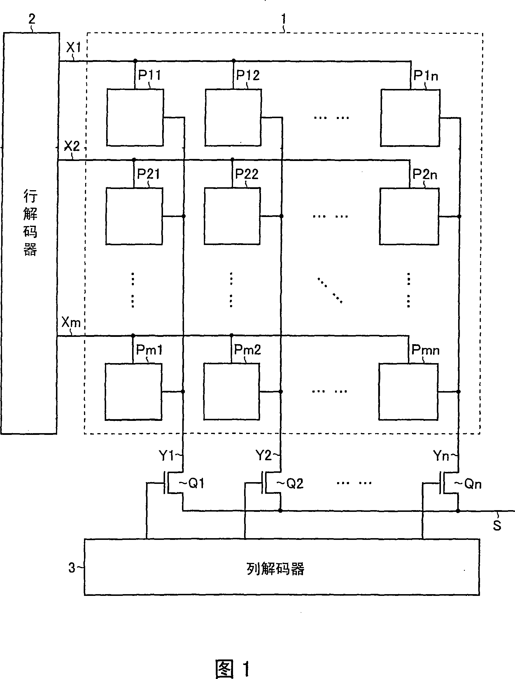
[0030] FIG. 1 is a block diagram showing an embodiment of a solid-state image sensing device according to the present invention.

[0031] As shown in the figure, the solid-state image sensing device of this embodiment includes a sensor array 1 , a row decoder 2 , and a column decoder 3 .

[0032] The sensor array 1 has row selection lines X1~Xm arranged in the horizontal direction and column selection lines Y1~Ym arranged in the vertical direction, and at the point where the row and column selection lines intersect, there are m×n (m, n each is an integer equal to or greater than 2) pixel sensors P11 to...


PUM


Abstract

A photoelectric conversion circuit has: a photoelectric conversion element that produces a detection current commensurate with the amount of light received thereby; a capacitor having one end connected to one end of the photoelectric conversion element, the one end of the capacitor from which a terminal voltage commensurate with the integral of the detection current is drawn; and an amplifier that receives the terminal voltage of the capacitor and produces an amplified signal commensurate with the terminal voltage thus received. The photoelectric conversion circuit outputs a final optical signal (an output current) by using the amplified signal of the amplifier. As a current path that can serve as a charging / discharging path of the capacitor, the photoelectric conversion circuit includes only a current path along which the photoelectric conversion element is located. With this configuration, it is possible to enhance responsivity to light and improve the S / N ratio of a received optical signal by making the most of electric power obtained from a photoelectric conversion element.

Description

technical field [0001] The present invention relates to a photoelectric conversion circuit and a solid-state image sensing device using the same. Background technique [0002] FIG. 5 is a circuit diagram showing one example of a CMOS (Complementary Metal Oxide Semiconductor) photoelectric conversion circuit (so-called CMOS sensor). [0003] In the illustrated CMOS sensor, the anode of the photodiode 51 is grounded, and the cathode of the photodiode 51 is connected to one end of the switch 54 . The other end of the switch 54 is connected to one end of the capacitor 52 , the gate of the N-channel field effect transistor 53 , and one end of the switch 55 , respectively. The other end of the capacitor 52 is grounded. The other end of the switch 55 is connected to a point to which the power supply voltage Vcc is applied. The drain of the transistor 53 is connected to a point to which the power supply voltage Vcc is applied. The source of the transistor 53 is connected to one ...

Claims


Application Information

Patent Timeline
Patent Type & Authority Applications(China)
IPC IPC(8): H04N5/335H04N3/15H01L27/146H04N5/357H04N5/369H04N5/374H04N5/376
CPCH04N5/357H04N3/155H04N3/1512H04N5/37452H04N25/60H04N25/771H04N25/77H04N25/76
Inventor 渊上贵昭守分政人
Owner ROHM CO LTD
Why Eureka
Try Eureka