Semiconductor device and fabrication method thereof

A semiconductor and substrate technology, applied in semiconductor/solid-state device manufacturing, semiconductor devices, radiation control devices, etc., can solve problems such as increasing S/N ratio and increasing RF signal noise

Inactive Publication Date: 2008-11-05
SONY CORP
View PDF0 Cites 9 Cited by
  • Summary
  • Abstract
  • Description
  • Claims
  • Application Information

AI Technical Summary

Problems solved by technology

[0006] The problem to be solved is because the circuit function of the existing photodiode integrated circuit is to convert the output of the photodiode by current / voltage (IV) and calculate the output to extract the focus tracking signal of the optical disc, and obtain the sum of these outputs as the The RF signal used as the data signal of the disc, so the noise of the RF signal increases, and thus increases the S / N ratio

Method used


Image

  • Semiconductor device and fabrication method thereof
  • Semiconductor device and fabrication method thereof
  • Semiconductor device and fabrication method thereof

Examples


Embodiment Construction

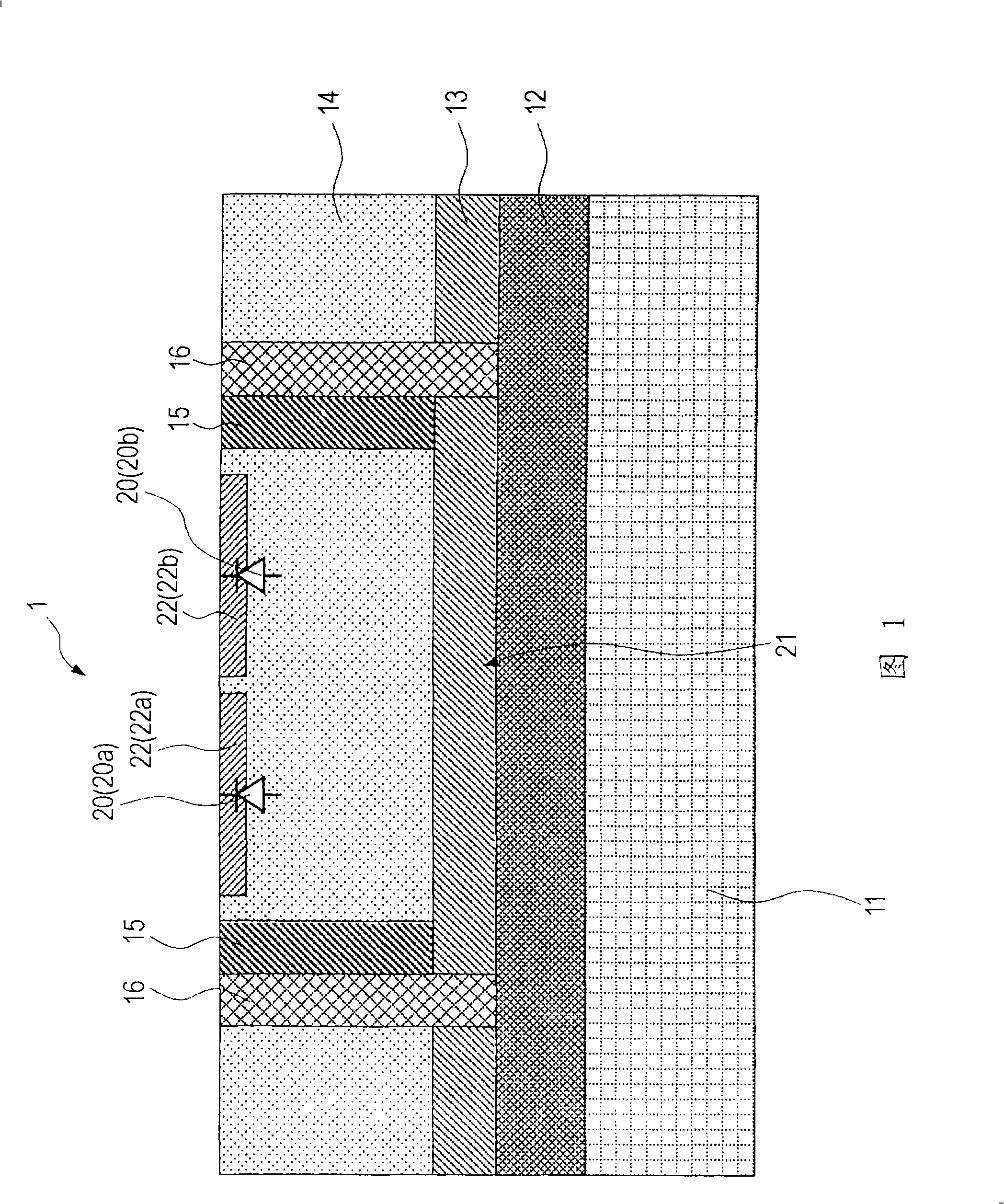
[0042] A first example of an embodiment of a semiconductor device according to the present invention is described with reference to a cross-sectional view of a schematic structure shown in FIG. 1 . FIG. 1 illustrates an example of a semiconductor device including a plurality of photodiodes electrically isolated from a semiconductor substrate employing an SOI (Silicon On Insulator) substrate.

[0043] As shown in FIG. 1 , an SOI (Silicon On Insulator) substrate is used in which an insulating layer 12 is formed on a semiconductor substrate 11 and a silicon layer is formed on the insulating layer 12 . The insulating layer 12 is formed of a silicon oxide film. P + Type impurities are introduced into the silicon layer. The silicon layer serves as the P + Type buried layer 13. For example, the impurity concentration of the buried layer 13 is set to be higher than or equal to 1×10 16 / cm 3 and less than or equal to 1×10 22 / cm 3 value. P - Type low concentration layer 14 is...


PUM


Abstract

A semiconductor device (1) has a plurality of photodiodes (20) on a semiconductor substrate (11). The photodiodes (20(20a, 20b)) have cathodes (22) and a common anode (21), which are formed electrically independent of the semiconductor substrate (11). In the photodiodes having the common anode (21) and the separated cathodes (22), the output from the common anode (21) is treated as equivalent to the sum of the outputs of the separated photodiodes (20). Alternatively, a plurality of photodiodes have a common cathode and a plurality of separated anodes, and the output from the common cathode is treated as equivalent to the sum of the outputs of the separated photodiodes. The anode and cathode of a photodiode are completely isolated electrically from the substrate, whereby noise and crosstalk can be reduced.

Description

technical field [0001] The present invention relates to a semiconductor device and a method of manufacturing the semiconductor device, and in particular, to a semiconductor device including a so-called photodetector integrated circuit and a method of manufacturing the same, a photodiode used as a photodetector device in the photodetector integrated circuit, and a semiconductor Integrated circuits such as bipolar integrated circuits or MOS integrated circuits are formed on the same semiconductor substrate. Background technique [0002] A semiconductor device including a photodetector integrated circuit (photodetector IC) is a semiconductor device in which a photosensitive diode used as a photodetector device converts light into electric current and performs signal processing such as IV (current to voltage) Transformation and matrix circuits. [0003] Next, a conventional photodetector IC semiconductor device will be described with reference to FIG. 24. FIG. [0004] As show...

Claims


Application Information

Patent Timeline
Patent Type & Authority Applications(China)
IPC IPC(8): H01L31/10H01L21/76H01L21/761H01L21/762H01L27/12H01L27/146
CPCH01L27/1443H01L21/76283H01L27/1203H01L27/14H01L27/1446H01L31/02024H01L31/10
Inventor 荒井千广
Owner SONY CORP
Why Eureka
Try Eureka