Photoconductive element

a photoconductive element and conductive technology, applied in the field of photoconductive elements, can solve the problems of difficult to increase resistance, increase the number of crystal defects, and inability to increase the application voltage, so as to improve the terahertz wave generation efficiency as well as the s/n

Active Publication Date: 2012-09-20
CANON KK
View PDF5 Cites 9 Cited by
  • Summary
  • Abstract
  • Description
  • Claims
  • Application Information

AI Technical Summary

Benefits of technology

[0009]It is therefore an object of the present invention to provide a structure for improving terahertz wave generation efficiency as well as the S / N ratio with the use of a low temperature growth layer.

Problems solved by technology

However, since an InGaAs system has a smaller band gap than that of GaAs, the carrier density of an intrinsic semiconductor is higher, and in addition the number of crystal defects is apt to increase because InGaAs is ternary.
Also owing to the increased residual carrier density, it is difficult to increase the resistance.
Therefore, the application voltage cannot be increased as compared to GaAs and it is difficult to increase the differential change of photocarriers, which limits terahertz wave generation efficiency.
The use of an InGaAs system as a detector increases a dark current to increase noise, which leads S / N ratio degradation.
9565 (2008), however, a heterointerface deteriorates when a low temperature grown film is exposed to high temperature, and it is difficult to increase the carrier trapping effect as designed.

Method used


Image

  • Photoconductive element
  • Photoconductive element
  • Photoconductive element

Examples


first embodiment

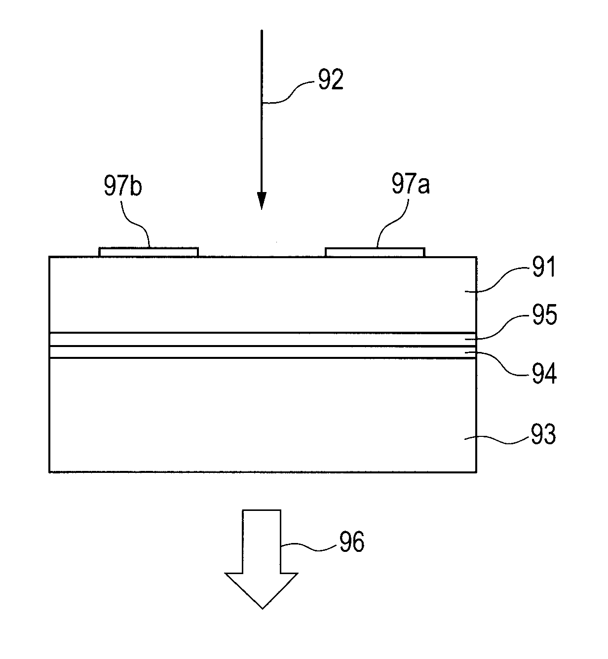
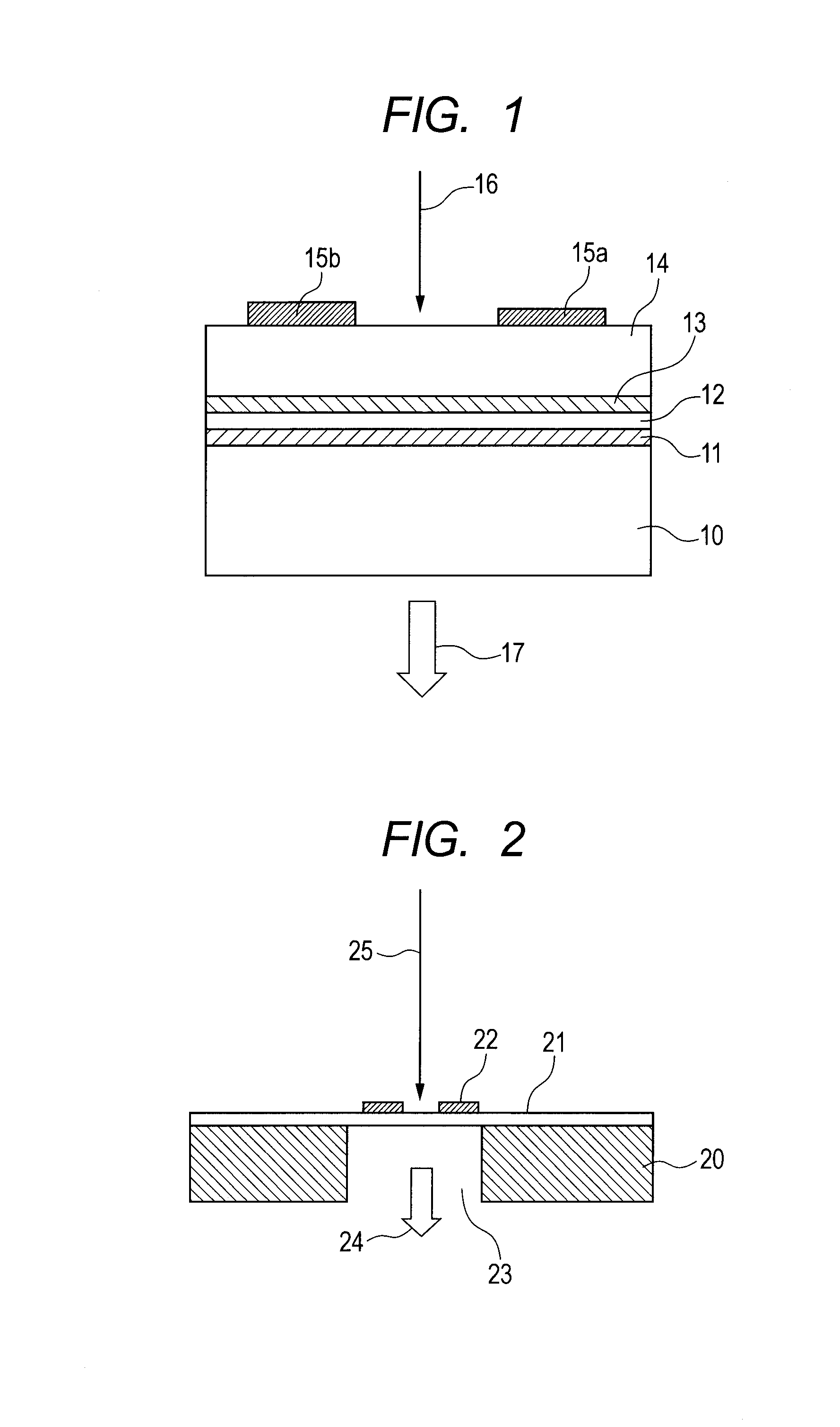
[0024]Referring to FIG. 1, a first embodiment of the present invention is described. In this embodiment, an InGaAs layer 11, an InAlAs layer 12, and an InGaAs layer 13 are formed on a semi-insulating InP substrate 10 at a normal growth temperature, and an LT-InGaAs layer 14 is formed thereon by low temperature growth as a semiconductor low temperature growth layer. In order to function as a photoconductive element, a pair of electrodes 15a and 15b also serving as an antenna is formed on the surface.

[0025]The semiconductor low temperature growth layer 14 generates a terahertz wave 17 by irradiation of laser light 16. In order to operate with light at a wavelength of, for example, 1.55 μm and to increase the resistance, the semiconductor low temperature growth layer 14 is doped with Be at 1018 cm−3 and grown at a growth temperature of 200° C. and further annealed at about 600° C. to enhance the crystallinity. The growth temperature of the semiconductor low temperature growth layer is ...

example 1

[0032]In Example 1 of the first embodiment, a layer that lattice-matches with an InP substrate (lattice constant: about 0.587 nm) is used. From a practical viewpoint of the element, a lattice-matched layer as used herein refers to a layer whose thickness does not exceed a critical thickness even if grown to be about several hundreds of nm or more in thickness, specifically, a layer which has the degree of lattice mismatch of 0.1% or less (see, for example, H. Komatsu ed., Handbook of Crystal Growth, Kyoritsu Shuppan, p. 699, 1995), and a lattice-mismatched layer refers to a layer which has a larger degree of lattice mismatch than 0.1%. In view of the above, the InGaAs layer 11, the InAlAs layer 12, and the InGaAs layer 13 were set to have In compositions of 0.53, 0.52, and 0.53 and thicknesses of 270 nm, 20 nm, and 5 nm, respectively. The semiconductor low temperature growth layer 14 was set to have an In composition of 0.53 and a thickness of 1.6 μm.

[0033]An example of configuring ...

example 2

[0037]Example 2 of the first embodiment is described. In this example, in order to more improve the resistivity, the In composition of the semiconductor low temperature growth layer 14 was set to 0.45. Although the band gap wavelength is 1.49 μm, since an electric field is applied for the function as a generating element, actually, laser light in the vicinity of 1.55 μm can also be absorbed.

[0038]In this case, the InGaAs layer 11 was set to have a total thickness of 270 nm, in which the thickness of a lattice-matched layer having an In composition of 0.53 was 250 nm and the thickness of a graded layer for reducing the In composition from 0.53 to 0.45 was 20 nm. The InAlAs layer 12 was 20 nm thick having an In composition of 0.45 (lattice constant: 0.584 nm). The InGaAs layer 13 was 5 nm thick having an In composition of 0.45 (lattice constant: 0.584 nm). Note that, the lattice constant values were determined according to the Vegard's law. In this case, the degree of lattice mismatch...


PUM

PropertyMeasurementUnit
temperatureaaaaaaaaaa
telecommunication wavelengthaaaaaaaaaa

Abstract

Provided is a photoconductive element which solves a problem inherent in an element for generating/detecting a terahertz wave by photoexcitation that terahertz wave generation efficiency is limited by distortions and defects of a low temperature grown semiconductor. The photoconductive element includes: a semiconductor substrate; a semiconductor low temperature growth layer; and a semiconductor layer, which is positioned between the semiconductor low temperature growth layer and the semiconductor substrate and is thinner than the semiconductor low temperature growth layer, in which the semiconductor low temperature growth layer includes a semiconductor which lattice-matches with the semiconductor layer and does not lattice-match with the semiconductor substrate.

Description

BACKGROUND OF THE INVENTION[0001]1. Field of the Invention[0002]The present invention relates to a photoconductive element, as exemplified by an element for generating / detecting (which means an element capable of at least one of generation and detection) an electromagnetic wave in a frequency region from millimeter wavebands to terahertz wavebands (30 GHz to 30 THz). More specifically, the present invention relates to an optical semiconductor element for generating / detecting an electromagnetic wave pulse containing a Fourier component in the frequency region by optical pulse irradiation, and to a terahertz time domain spectroscopy apparatus using the optical semiconductor element.[0003]2. Description of the Related Art[0004]In recent years, non-destructive sensing technology using an electromagnetic wave ranging from millimeter waves to terahertz (THz) waves (30 GHz to 30 THz; hereinafter, also referred to simply as terahertz wave) has been developed. In the application field of the...

Claims


Application Information

Patent Timeline
Patent Type & Authority Applications(United States)
IPC IPC(8): G01J3/28H01L31/18H01L31/12G01J1/02G01N21/35G01N21/3586H01L21/205H01L31/0264H01S1/02
CPCG01J3/42G01N21/3586H01L31/09
Inventor OUCHI, TOSHIHIKOKAJIKI, KOUSUKE
Owner CANON KK
Why Eureka
Try Eureka