Optical member holding device, semiconductor laser device, method of manufacturing optical member holding device, and method of manufacturing semiconductor laser device

a semiconductor laser and optical member technology, applied in semiconductor lasers, laser details, electrical devices, etc., can solve the problems of reducing reliability in heat-resistance properties, mechanical strength, other properties, etc., and achieve high reliability, mechanical strength, and high precision positioning

Active Publication Date: 2019-05-16
NICHIA CORP
View PDF2 Cites 4 Cited by
  • Summary
  • Abstract
  • Description
  • Claims
  • Application Information

AI Technical Summary

Benefits of technology

[0010]According to the present disclosure, an optical member holding device and a semiconductor laser device having high reliability in terms of heat-resisting properties and mechanical strength can be provided. Also, the present disclosure can provide a method of manufacturing an optical member holding device or a semiconductor laser device in which an optical member can be disposed without highly precise positioning to a holding member.

Problems solved by technology

However, the engaging part of such a conventional optical unit consists of a thermoplastic resin (i.e., organic material) that may reduce reliability in terms of heat-resisting property, mechanical strength, and other properties.

Method used


Image

  • Optical member holding device, semiconductor laser device, method of manufacturing optical member holding device, and method of manufacturing semiconductor laser device
  • Optical member holding device, semiconductor laser device, method of manufacturing optical member holding device, and method of manufacturing semiconductor laser device
  • Optical member holding device, semiconductor laser device, method of manufacturing optical member holding device, and method of manufacturing semiconductor laser device

Examples


first embodiment

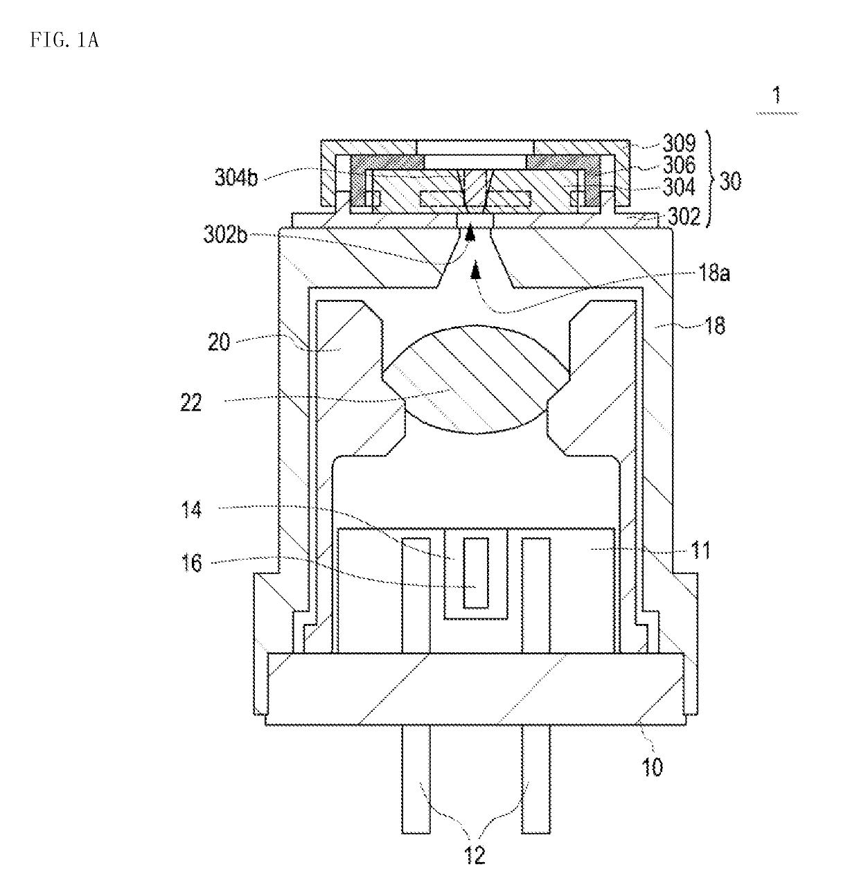
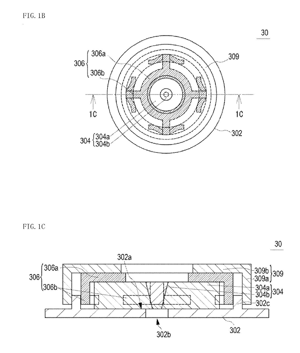
[0033]FIG. 1A is a schematic cross-sectional view of a semiconductor laser device 1 according to a first embodiment of the present invention. FIG. B is a schematic plan view of an optical member holding device 30 according to the first embodiment, and FIG. 1C is a cross sectional view taken along line 1C-1C in FIG. 1B. In FIG. 13B, hatching is used to indicate an elastic member 306. In the cross-sectional views and the plan views, portion(s) of member(s) shown through other member(s) are illustrated by broken lines to clarify the configuration of the members.

[0034]As shown in FIG. 1A, the semiconductor laser device 1 includes a base 10, a semiconductor laser element 16 disposed above the base 10, a cover 18 disposed above the base 10, and an optical member holding device 30. The cover 18 has an upper surface defining a through-hole 18a to allow light from the semiconductor laser element 16 to pass through. The optical member holding device 30 is disposed above the cover 18 such that...

second embodiment

[0094]FIG. 6A is a schematic cross-sectional view of a semiconductor laser device 2 according to a second embodiment of the present invention. FIG. 6B is a schematic plan view of an optical member holding device 30 according to the second embodiment, and FIG. 6C is a cross sectional view taken along line 6C-6C in FIG. 6B. In FIG. 6B, hatching is used to indicate an elastic member 307. FIG. 7A is a schematic plan view of the elastic member 307 according to the second embodiment, and FIG. 7B is a cross sectional view taken along line 7B-7B in FIG. 7A. In FIG. 7A, hatching is used to indicate supporting parts 307b.

[0095]As shown in FIG. 6A to FIG. 7B, the semiconductor laser device 2 according to the second embodiment differs from the semiconductor laser device 1 according to the first embodiment, in that, the supporting parts 307b of the elastic member 307 are bent downward and subsequently bent inwardly upward. In other words, each of the supporting parts 307b includes a distal end ...


PUM


Abstract

An optical member holding device includes a holding member, an optical member and an elastic member. The holding member has a recess defined by one or more lateral surfaces and a bottom surface with a through-hole opening at the bottom surface. The optical member is disposed on the bottom surface of the recess, and includes a light transmissive part. The optical member has an upper surface and one or more lateral surfaces. The elastic member consists of an inorganic material. The elastic member includes a main part disposed on the upper surface of the optical member, and a plurality of supporting parts each extending outward and bending downward to be in contact with the one or more lateral surfaces of the recess and the one or more lateral surfaces of the optical member to exert elastic force that secures the optical member in a predetermined location in the recess.

Description

CROSS-REFERENCE TO RELATED PATENT APPLICATION[0001]The present application claims priority under 35 U. S. C. § 119 to Japanese Patent Application No. 2017-219238, filed Nov. 14, 2017. The contents of Japanese Patent Application No. 2017-219238 are incorporated herein by reference in their entirety.BACKGROUNDTechnical Field[0002]The present disclosure relates to an optical member holding device, a semiconductor laser device, a method of manufacturing the optical member holding device, and a method of manufacturing the semiconductor laser device.Description of Related Art[0003]There has been proposed an optical unit having an optical member, a holding member to hold the optical member, and an engaging part to be fit in a recess formed in an outer circumference of the optical member or in an inner circumference of the holding member. In order to firmly fix the optical member to the holding member, the engaging part is irradiated with a laser light and melted to weld the optical member ...

Claims


Application Information

Patent Timeline
Patent Type & Authority Applications(United States)
IPC IPC(8): H01S5/022H01S5/02315H01S5/0233
CPCH01S5/02296H01S5/02236H01S5/02212H01S5/02469H01S5/02326H01S5/02257H01S5/0087H01S5/02315H01S5/0233H01S5/0235H01S5/005
Inventor KURODA, HIROAKIMIYOSHI, TOMONORI
Owner NICHIA CORP
Why Eureka
Try Eureka