Filter Circuit with Programmable Gain and Frequency Response

a filter circuit and frequency response technology, applied in the direction of filters, tunable filters, gated amplifiers, etc., can solve the problems of large power consumption, difficult to implement simultaneous and difficult to implement gain control and frequency tuning. , to achieve the effect of simple implementation of the output converter, simple controllability of the gain, and easy implementation of the proportionality constan

Active Publication Date: 2019-05-23
HUAWEI TECH CO LTD
View PDF3 Cites 1 Cited by
  • Summary
  • Abstract
  • Description
  • Claims
  • Application Information

AI Technical Summary

Benefits of technology

[0027]According to a further implementation form of the previous implementation form, the first current extraction element comprises a first current extraction transistor, the second current extraction element comprises a second current extraction transistor. A base of the first current extraction transistor is connected to a base of the second current extraction transistor. An emitter of the second current extraction transistor is connected to a resistive element, the value of the resistive element setting the proportionality constant. It is thereby very easily possible to implement the proportionality constant in the circuit.
[0028]According to a further implementation form of the first aspect or any of the previously described implementation forms, the input signal is a differential signal, the first output current signal is a differential signal, and the filter comprises two current extraction transistors, forming a differential current extraction pair configured to extract the first output current signal from the filter. The first amplified current signal therefore is also a differential signal, as well as the output signal. It is thereby possible to handle differential signals by the filter circuit,
[0029]According to a further implementation form, the first Current mirror element is a first controllable differential transistor pair and the second current mirror element is a second controllable differential transistor pair, the first and the second controllable differential transistor pair being controllable to adjust a gain of the filter circuit and / or the first controllable differential transistor pair and the second controllable differential transistor pair are configured to jointly generate the amplified current signal. This allows for a very simple controllability of the gain.
[0030]According to a further implementation form of the previously described implementation forms, the current-to-voltage converter comprises at least one resistor configured to convert the amplified current signal to the output signal. This allows for a very simple implementation of the output converter.
[0031]According to a further implementation form of the previously described implementation forms, the amplified current signal and the output signal are differential signals. The current-to-voltage converter comprises a first resistor and a second resistor, each connected to ground. The differential component signals of the amplified current signal are each connected to one of the first resistor and the second resistor. Each of the first resistor and the second resistor converts the respective component of the amplified current signal into a corresponding component of the output signal. This allows for a very simple to implement output converter for differential signals.
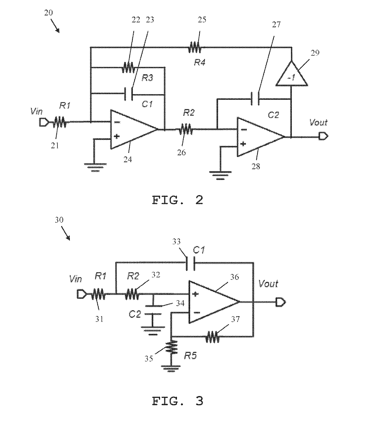
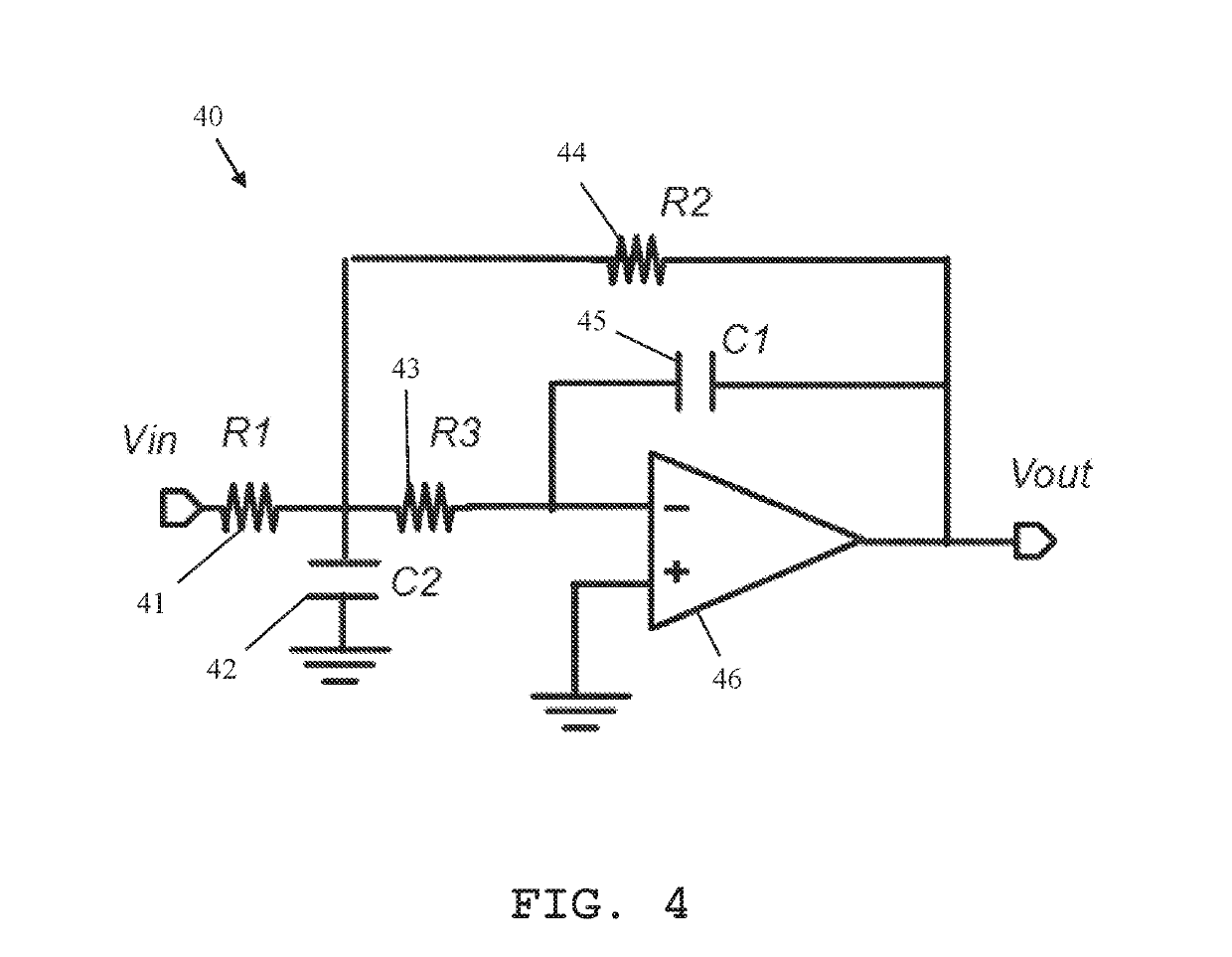
[0032]According to a further implementation form of the first aspect or any of the previously described implementation forms, the filter is a high-pass filter or a band-pass filter or a low-pass filter and the filter is a Sallen-Key filter or an MFB filter. This allows for an especially simple-to-implement filter construction.

Problems solved by technology

Further, it is difficult to implement gain control and frequency tuning.
The BiQuad filter requires two operational amplifiers and therefore consumes a large amount of power.
With the MFB filter is difficult to implement simultaneous gain control and frequency tuning.
This disadvantage, i.e. it is not possible to control simultaneously gain and frequency, makes it necessary to use a separate PGA in case a programmable gain control is needed, like in a typical wireless communication system, as shown in the following FIGS. 5 and 6.
Both alternatives have the joint disadvantage of the extra programmable gain amplifier 51, 62 drawing extra current and reducing system bandwidth.

Method used


Image

  • Filter Circuit with Programmable Gain and Frequency Response
  • Filter Circuit with Programmable Gain and Frequency Response
  • Filter Circuit with Programmable Gain and Frequency Response

Examples


Embodiment Construction

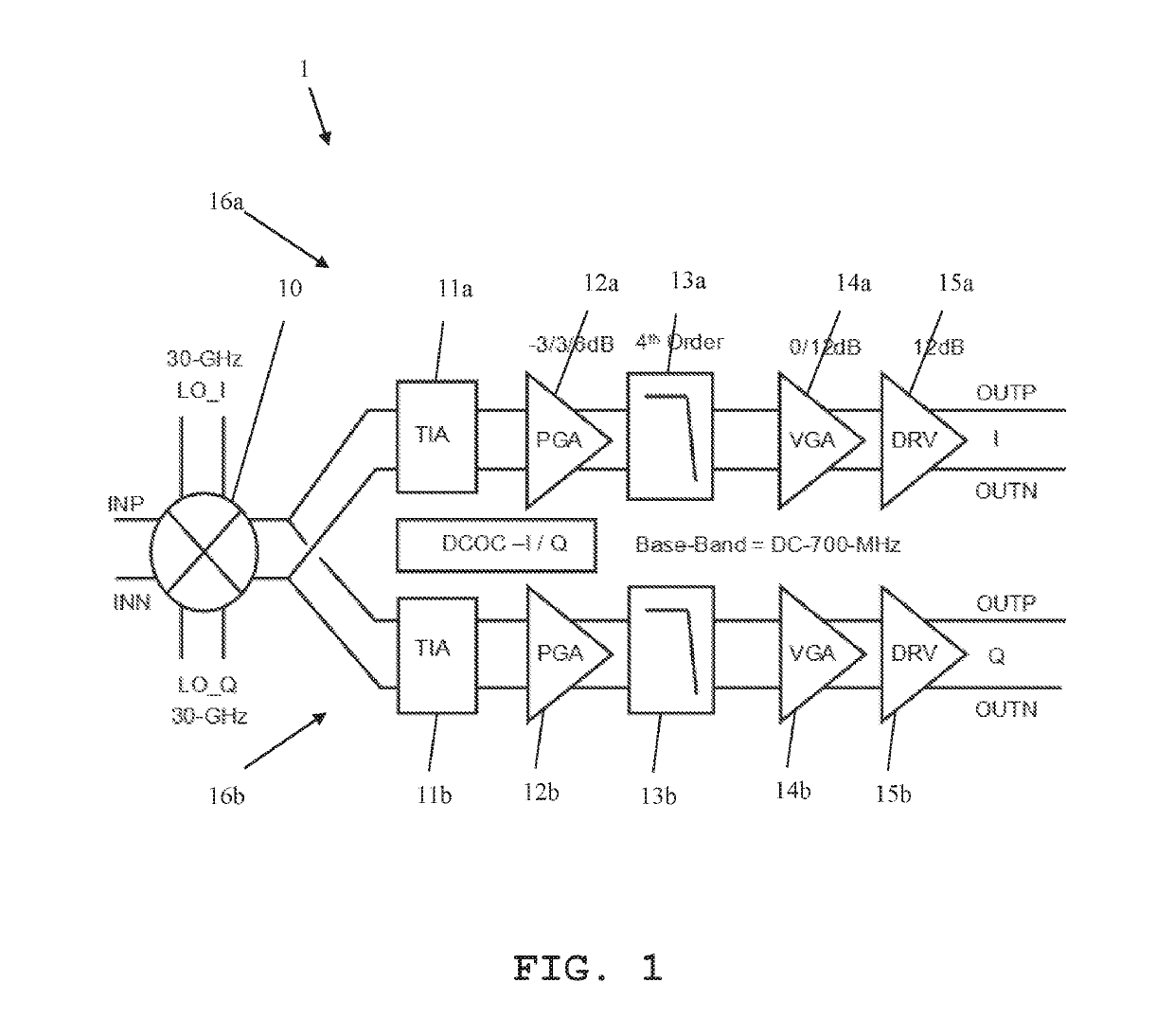
[0048]First, the underlying problem and exemplary filter structures and filter circuits have been described along FIG. 1-FIG. 6. In the following, along FIG. 7, a general construction of a filter circuit according to the first aspect of the disclosure is described. Along FIG. 8-FIG. 14, different embodiments of the filter circuit of the first aspect of the disclosure are shown. Similar entities and reference numbers in different figures have been partially omitted.

[0049]In FIG. 7, a filter circuit 70 according to the first aspect of the disclosure is shown. The filter circuit 70 comprises a filter 72 and a current mode programmable gain amplifier 74. The filter 72 is connected to the current mode programmable gain amplifier 74. The filter 72 moreover comprises a current extraction element 73.

[0050]An input signal VF_IN+, VF_IN− is provided to the filter circuit 70, especially to the filter 72. A filtering of the input signal 71 is performed by the filter 72. The current extraction e...


PUM


Abstract

A filter circuit includes a filter and a current mode programmable gain amplifier, where the filter circuit is configured to filter an input signal to obtain an output signal. The filter is supplied with the input signal. The filter comprises at least one current extraction element configured to extract a first output current signal. The current mode programmable gain amplifier is configured to receive and amplify the first output current signal to obtain an amplified current signal. The output signal is derived from the amplified current signal.

Description

CROSS-REFERENCE TO RELATED APPLICATIONS[0001]This application is a continuation of International Patent Application No. PCT / EP2016 / 071688 filed on Sep. 14, 2016, which is hereby incorporated by reference in its entirety.TECHNICAL FIELD[0002]The disclosure relates to a filter for filtering high frequency signals, especially communications signals.BACKGROUND[0003]A typical scheme for a wireless communications in the RX section is shown in FIG. 1. The circuit 1 comprises a mixer 10, which is connected to two processing paths 16a, 16b. Both processing paths 16a, 16b each comprise an input processing network 11a, 11b, connected to a programmable gain amplifier (also referred to as PGA) 12a, 12b, which in turn is connected to a low-pass filter 13a, 13b. The low-pass filters 13a, 13b are each connected to a variable gain amplifier 14a, 14b, which in turn is connected to a driver 15a, 15b. [0004]A differential input signal INP, INN is entered into the mixer 10 and mixed with a local oscilla...

Claims


Application Information

Patent Timeline
Patent Type & Authority Applications(United States)
IPC IPC(8): H03H11/12H03F3/45H03F3/72
CPCH03H11/1286H03H11/1291H03F3/45197H03F3/72H03H2210/017H03H11/126H03H2210/012H03H11/12
Inventor GRAMEGNA, GIUSEPPE
Owner HUAWEI TECH CO LTD
Why Eureka
Try Eureka