System and method for correcting offset voltage errors within a band gap circuit

a band gap circuit and offset voltage technology, applied in the direction of electric variable regulation, process and machine control, instruments, etc., can solve the problems of significant area penalty, reduce the accuracy of band gap voltage, achieve a high level of accuracy, etc., and achieve the effect of minimizing the offset voltage error of the error amplifier

Active Publication Date: 2019-06-06
SILICON LAB INC
View PDF3 Cites 6 Cited by
  • Summary
  • Abstract
  • Description
  • Claims
  • Application Information

AI Technical Summary

Benefits of technology

[0004]A band gap circuit with offset voltage error correction according to one embodiment includes a diode junction circuit, an error amplifier, a current device, a bias current generator, a calibration circuit, and a mode control circuit. The diode junction circuit includes an input node, a first feedback node, and a second feedback node, in which the diode junction circuit includes proportional and complimentary temperature coefficients when the first and second feedback nodes are driven to a common voltage level. The error amplifier has a positive input coupled to the second feedback node, has a negative input coupled to the first feedback node, has an output, and has at least one trim node. The current device has a control terminal coupled to the output of the error amplifier and has an output that provides a control current during a normal mode. The bias current generator with constant gain sinks a first bias current and sources a second bias current. The calibration circuit monitors the output of the current device while adjusting a trim current provided to the at least one trim node of the error amplifier to minimize an offset voltage error of the error amplifier during a calibration mode. The mode control circuit couples the current device to the input node to provide the control current to the diode junction circuit during the normal mode, and periodically enters the calibration mode during which the mode control circuit decouples the current device from the diode junction circuit, shorts together the positive and negative inputs of the error amplifier, and couples the current generator to sink the first bias current from the output of the current device and to source the second bias current to the input node of the diode junction circuit.

Problems solved by technology

The error amplifier, however, may have an input referred offset voltage error which, if not corrected, reduces the accuracy of the band gap voltage.
The auto-zero technique, however, could only achieve a high level of accuracy with the use of very large capacitors, which resulted in a significant area penalty.
The offset-nulling technique also did not correct for offset voltage variations over time.
High end laser trimming techniques are expensive and only provided a one-time permanent trim that did not correct for offset voltage error variations over time.

Method used


Image

  • System and method for correcting offset voltage errors within a band gap circuit
  • System and method for correcting offset voltage errors within a band gap circuit
  • System and method for correcting offset voltage errors within a band gap circuit

Examples


Embodiment Construction

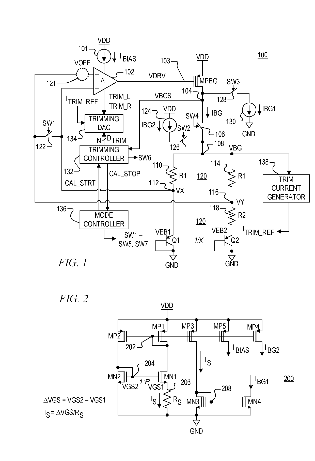
[0023]The inventors have recognized the need to provide a substantially fixed band gap voltage that develops and maintains a high level of accuracy over time. The term “fixed” as used herein is defined as invariable or unchanging in spite of circuit variables, such as temperature changes, power supply voltage changes, and manufacturing process variables. They have therefore developed a system and method for correcting the offset voltage error of an error amplifier used within a band gap (BG) circuit providing the band gap voltage. The BG circuit includes a diode junction circuit, the error amplifier, and a current device, in which the diode junction circuit includes an input node and a pair of feedback nodes. During a normal mode of operation, the error amplifier drives the current device to provide a BG current to the input node to keep the feedback nodes at a common voltage level. In one embodiment, the input node develops the band gap voltage, in which case the diode junction cir...


PUM


Abstract

A band gap circuit with offset voltage error correction including a diode junction circuit, an error amplifier, a current device, a bias current generator, a calibration circuit, and a mode control circuit. During a normal mode of operation, the error amplifier monitors feedback nodes of the diode junction circuit and drives the current device to provide a control current to the diode junction circuit. During a calibration mode, the current device is decoupled from the diode junction circuit and the inputs of the error amplifier are shorted together, the bias generator circuit sinks a bias current from the current device and separately sources a bias current to the diode junction circuit such that the error amplifier operates as a comparator, and the calibration circuit monitors the output of the current device while adjusting a trim current of the error amplifier to minimize an offset voltage error of the error amplifier.

Description

BACKGROUND OF THE INVENTIONField of the Invention[0001]The present invention relates in general to error amplifier offset correction, and more particularly to a system and method for correcting an offset voltage error of an error amplifier used within a band gap circuit that provides a band gap voltage.Description of the Related Art[0002]A band gap circuit provides a fixed band gap voltage that is relatively independent of one or more circuit variables, including, for example, temperature changes, power supply voltage changes, and manufacturing process variables. The band gap voltage is typically used by various devices in the circuit, such as regulators and converters (analog to digital or vice-versa) and the like, so that accuracy of the band gap voltage is often critical to proper circuit operation and / or maximum performance. The band gap circuit may include an error amplifier in a closed loop configuration that establishes or maintains at least one circuit control parameter to e...

Claims


Application Information

Patent Timeline
Patent Type & Authority Applications(United States)
IPC IPC(8): G05F1/575G05F1/565
CPCG05F1/575G05F1/565G05F3/242G05F3/30
Inventor ELSAYED, MOHAMEDWILLINGHAM, SCOTT D.
Owner SILICON LAB INC
Why Eureka
Try Eureka