Operational amplifier circuit structure

a circuit structure and amplifier technology, applied in the field of operational amplifiers, can solve the problems of undermining the performance of the traditional operational amplifier device, discrepancy between input voltage and output voltage, and almost impossible to achieve the above-mentioned characteristics of the real-world operational amplifier, and achieve the effect of minimizing offset voltage and larger gain

Inactive Publication Date: 2014-04-15
INTEGRATED SOLUTIONS TECH
View PDF1 Cites 1 Cited by
  • Summary
  • Abstract
  • Description
  • Claims
  • Application Information

AI Technical Summary

Benefits of technology

[0010]The primary objective of the instant disclosure is to provide an operational amplifier circuit structure that is capable of minimizing the offset voltage and providing a larger gain.
[0012]For minimizing an occurrence of an offset voltage, the first current mirror ratio and the second current mirror ratio may be adjusted to be substantially the same, causing the first output impedance and the second impedance to be substantially the same.

Problems solved by technology

However, due to limitations to the manufacturing process of the operational amplifiers it is almost impossible for the real-world operational amplifiers to possess the above-mentioned characteristics.
Thus, the changes in the output voltage could not synchronize with the changes in the input voltage, resulting in discrepancy between the input voltage and the output voltage at least at certain points of time.
Consequently, the voltage stored in the capacitor may not be equal to the offset voltage and cannot be entirely compensated when the traditional operational amplifier device operates in the offset voltage compensating mode, undermining the performance of the traditional operational amplifier device.

Method used


Image

  • Operational amplifier circuit structure
  • Operational amplifier circuit structure
  • Operational amplifier circuit structure

Examples


first embodiment

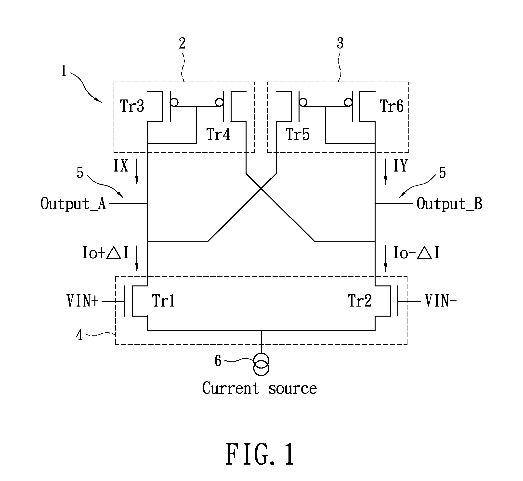
[0023]Please refer to FIG. 1 illustrating an operation amplifier circuit structure 1 according to the instant disclosure. The operation amplifier circuit structure 1 may include a first current mirror 2, a second current mirror 3, an input portion 4, an output portion 5, and a current source 6. The input portion 4 may be implemented in terms of a pair of transistors Tr1 and Tr2, while the first current mirror 2 may be formed by another pair of transistors Tr3 and Tr4 having a mirror ratio of α. Meanwhile, the second current mirror 2 may be formed by another pair of transistors Tr5 and Tr6 having a mirror ratio of β.

[0024]Sources of the transistors Tr3 and Tr5 may be coupled to a drain of the transistor Tr1, gates of the transistors Tr3 and Tr4 may be coupled to each other, and gates of the transistors Tr5 and Tr6 may be coupled to each other as well. At the same time, sources of the transistors Tr4 and Tr6 may be coupled to a drain of the transistor Tr2, and source of the transistor...

second embodiment

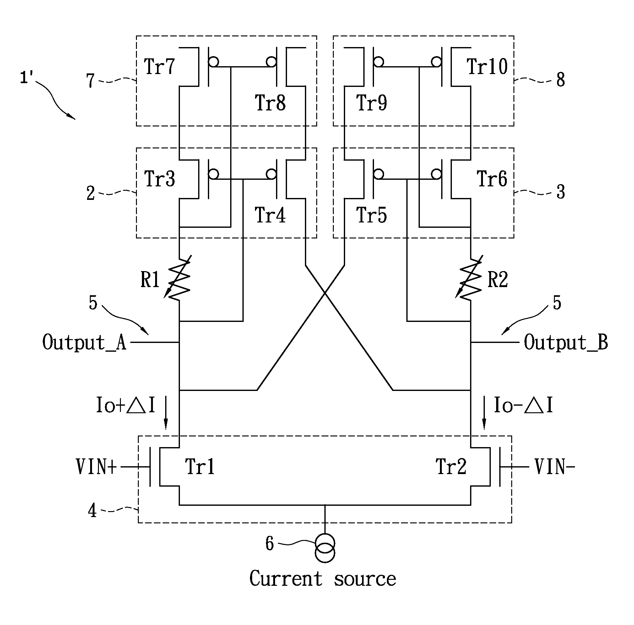
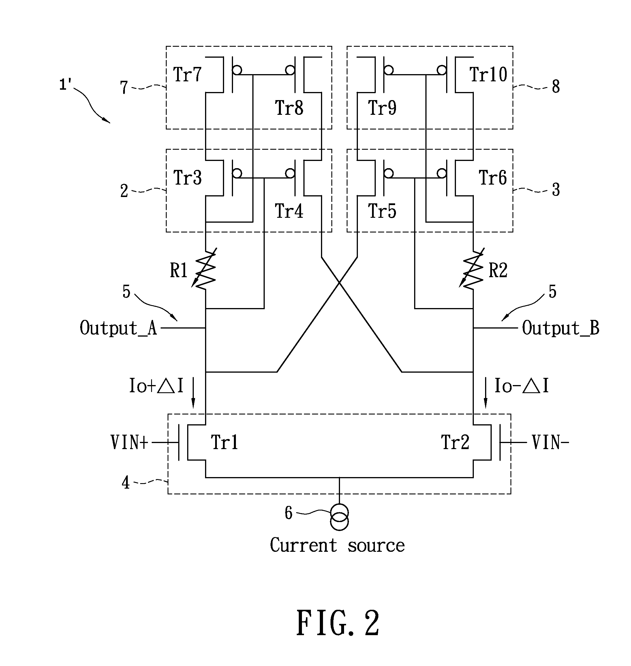
[0033]Please refer to FIG. 2 of a simplified circuit diagram of another operational amplifier circuit structure 1′ according to the instant disclosure. Compared with the operational amplifier circuit structure 1, the operational amplifier circuit structure 1′ may further include a third current mirror 7 and a fourth current mirror 8. The third current mirror 7 may be associated with a third current mirror ratio of K, while the fourth current mirror 8 may be associated with a fourth current mirror ratio of K. As previously mentioned, in one implementation the third current mirror ratio and the fourth current mirror ratio may be the same as the current mirror ratios of the first current mirror and the second current mirror. Meanwhile, the third current mirror 7 may be coupled to the first current mirror 2 at a predetermined location that is on the same side along with the input portion 4. The fourth current mirror 8 may be coupled to the second current mirror 3 at another predetermine...

third embodiment

[0041]Please refer to FIG. 4 illustrating a simplified circuit diagram of an operational amplifier circuit structure 1″ according to the instant disclosure. As shown in FIG. 4, an input portion 4 may be implemented in terms of a rail-to-rail amplifier circuit having a PMOS and a NMOS, with transistors Tr11 to Tr30 and variable resistance R3 to R6.

[0042]The variable resistance R3 to R6 may be coupled to gates of cascade current mirrors having the transistors Tr13 / Tr14, Tr15 / Tr16, Tr17 / Tr18, and Tr19 / Tr20, respectively, for ensuring the offset voltages of the current mirrors may be compensated and broader dynamic ranges.


PUM


Abstract

An operational amplifier circuit structure is provided. The operational amplifier circuit structure includes a first current mirror associated with a first current mirror ratio, a second current mirror coupled to the first current mirror and associated with a second current mirror ratio, an input portion coupled to the first current mirror and the second current mirror, an output portion coupled between the input portion and the first current mirror and the input portion and the second current mirror, and associated with a first output impedance and a second output impedance, respectively, and a current source coupled to the input portion.

Description

BACKGROUND OF THE INVENTION[0001]1. Field of the Invention[0002]The instant disclosure relates to an operational amplifier, and more particularly, to an operational amplifier that is capable of minimizing impact of an offset voltage by adjusting a gain thereof through manipulation of a current mirror ratio of a current mirror and a load.[0003]2. Description of Related Art[0004]Operational amplifiers have been widely utilized in numerous electronic components such as buffers, filters, and digital-to-analog converters.[0005]Ideal operational amplifiers are associated with characteristics including infinite input resistance, zero output impedance, infinite open loop gain, infinite common mode rejection ratio, and indefinite bandwidth. However, due to limitations to the manufacturing process of the operational amplifiers it is almost impossible for the real-world operational amplifiers to possess the above-mentioned characteristics. And the deviation from the ideality is traditionally r...

Claims


Application Information

Patent Timeline
Patent Type & Authority Patents(United States)
IPC IPC(8): H03F3/45
CPCH03F3/45183H03F2203/45686H03F2203/45644H03F2203/45651H03F3/211H03F2203/45652H03F3/3022H03F2203/45658
Inventor LIN, PO-CHIH
Owner INTEGRATED SOLUTIONS TECH
Why Eureka
Try Eureka