System and method for providing an offset voltage minimization circuit

a technology of offset voltage and minimization circuit, which is applied in the field of integrated circuits, can solve the problems of significantly affecting the output accuracy of switching power supply circuit, significantly affecting the matching of cmos transistors, and reducing accuracy, so as to achieve efficient minimizing the offset voltage

Active Publication Date: 2009-04-28
NAT SEMICON CORP
View PDF13 Cites 8 Cited by
  • Summary
  • Abstract
  • Description
  • Claims
  • Application Information

AI Technical Summary

Benefits of technology

[0018]To address the above-discussed deficiencies of the prior art, it is a primary object of the prese

Problems solved by technology

This particular problem is much worse with complementary metal oxide semiconductor (CMOS) amplifiers because the matching of the CMOS transistors is significantly poorer than the matching of similarly sized bipolar transistors.
These offset errors (and the resulting temperature drift) can significantly affect the output accuracy of a switching power supply circuit.
These offset errors may decrease the accuracy from a level of one percent (1%) over temperature to a level of five percent (5%) over temperature.
The primary source of error in the reference voltage (VREF) is due to the bandgap error amplifier 120 that is used to drive the bandgap core.
The problem is again much worse in CMOS transistor switching power supply circuits because of the previously mentioned poor matching of CMOS transistors and because of a lack in many technologies of quality 3 terminal bipolar transistors (that have improved matching characteristics).
Even a small offset voltage in the error amplifier (A1) can cause a big error in the bandgap voltage (VBG).
This, in turn, can cause a poor voltage reference temperature coefficient because the bandgap is not biased at the correct voltage for the ideal temperature coefficient.
There are always initial errors due to the mismatch between the critical matching transistors of the error amplifier (A1) and the resulting degraded temperature performance.
In addition to these initial errors, there are also very significant errors attributed to the assembly shift of the integrated circuit chip.
The errors that result at the reference output voltage are very significant becau

Method used


Image

  • System and method for providing an offset voltage minimization circuit
  • System and method for providing an offset voltage minimization circuit
  • System and method for providing an offset voltage minimization circuit

Examples


Embodiment Construction

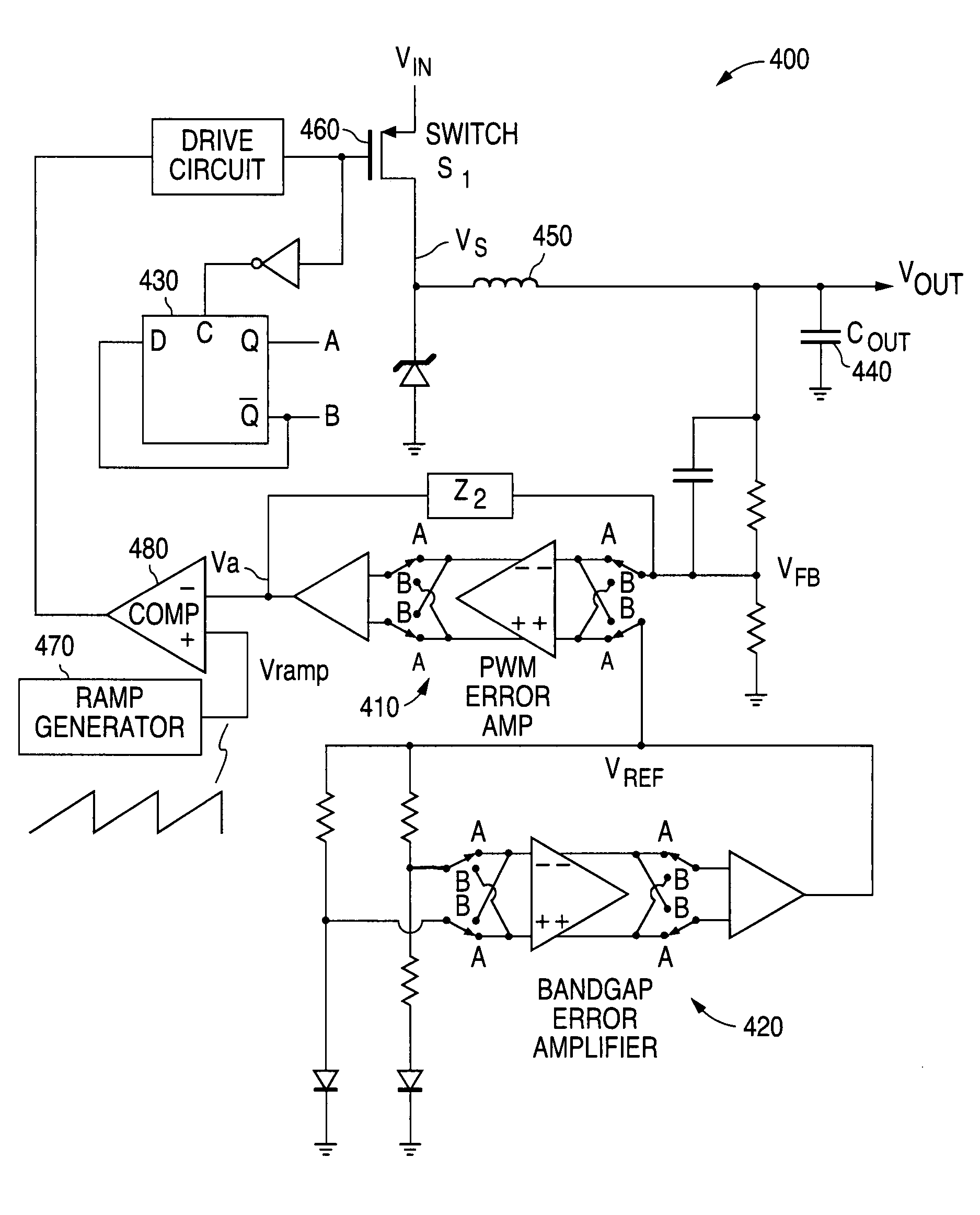
[0035]FIGS. 3 through 7, discussed below, and the various embodiments used to describe the principles of the present invention in this patent document are by way of illustration only and should not be construed in any way to limit the scope of the invention. Those skilled in the art will understand that the principles of the present invention may be implemented in any type of suitably arranged semiconductor device.

[0036]Specifically, the offset voltage minimization circuit of the present invention will be described in connection with a switching power supply circuit. It is understood that the offset voltage minimization circuit of the present invention is not limited to use in switching power supply circuits but may also be used in other types of circuits that employ an inductor / capacitor filter circuit at the output that is capable of averaging the effects of switching between two offsets.

[0037]Because a switching power supply circuit has a regular repetitive period during normal o...


PUM


Abstract

A system and method is disclosed for providing an offset voltage minimization circuit for an amplifier circuit. The present invention comprises a flip flop zero amplifier circuit that is capable of operating in a first configuration during a first period of time to obtain a first value of offset voltage. The flip flop zero amplifier circuit is also capable of operating in a second configuration during a second period of time to obtain a second value of offset voltage that has a polarity that is opposite to that of the first value of offset voltage. The two values of offset voltage are then averaged to obtain an average value of offset voltage that is approximately zero volts. The invention may be advantageously employed in a switching power supply circuit.

Description

TECHNICAL FIELD OF THE INVENTION[0001]The present invention relates generally to integrated circuits and, more particularly, to a system and method for providing an offset voltage minimization circuit.BACKGROUND OF THE INVENTION[0002]A major goal in the design and manufacture of electronic circuitry is to increase the accuracy and precision of the operation of integrated circuits. In some instances the accuracy and precision of an integrated circuit may be increased by minimizing the error that is present in an input signal to an amplifier circuit. For example, consider the operation of a switching power supply circuit such as a direct current (DC) to direct current (DC) switching regulator. A block diagram of an exemplary prior art voltage mode compensation switching power supply circuit 100 is illustrated in FIG. 1.[0003]The precision of voltage mode compensation switching power supply circuit 100 is limited by the accuracy of the internal voltage reference (VREF) and the input er...

Claims


Application Information

Patent Timeline
IPC IPC(8): H03L5/00
CPCH02M3/156H03F3/45475
Inventor HENRY, PAUL MICHAEL
Owner NAT SEMICON CORP
Why Eureka
Try Eureka