

Circuit adapter board
- Summary
- Abstract
- Description
- Claims
- Application Information
AI Technical Summary
Benefits of technology
Problems solved by technology
Method used
Image

Examples
first embodiment
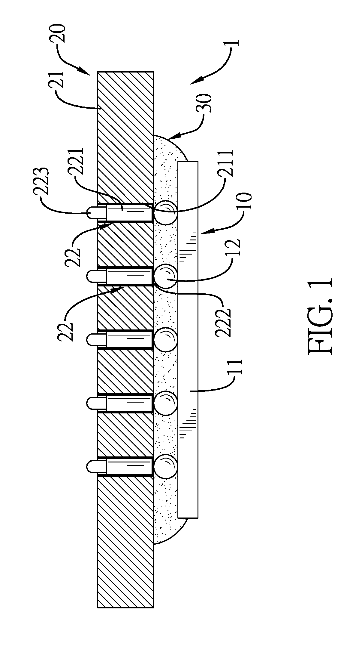
[0022]With reference to FIG. 1, a circuit adapter board 1 in accordance with the present invention comprises a film circuit board 10, a spring probe assembly 20, a space, and a filler 30.
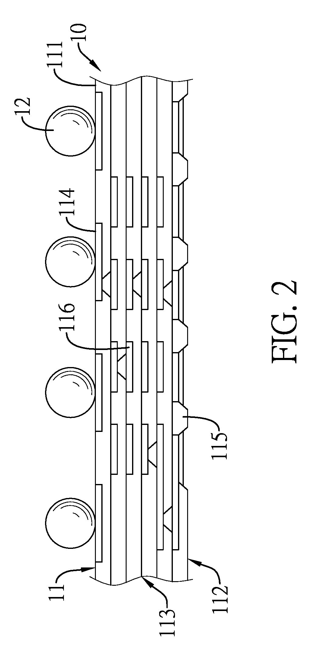
[0023]With reference to FIGS. 1 and 2, the film circuit board 10 has a film body 11 and multiple conductors 12. The film body 11 is a slim sheet and has a first outer layer 111, a second outer layer 112, and an inner layer 113. The first outer layer 111 has an outer surface, an inner surface, and multiple first contacts 114. The inner surface of the first outer layer 111 is opposite to the outer surface of the first outer layer 111. The first contacts 114 are disposed in the first outer layer 111 at spaced intervals and exposed out of the outer surface of the first outer layer 111. The second outer layer 112 is opposite to the first outer layer 111 and has an outer surface, an inner surface, and multiple second contacts 115. The inner surface of the second outer layer 112 is opposite to the outer su...
second embodiment
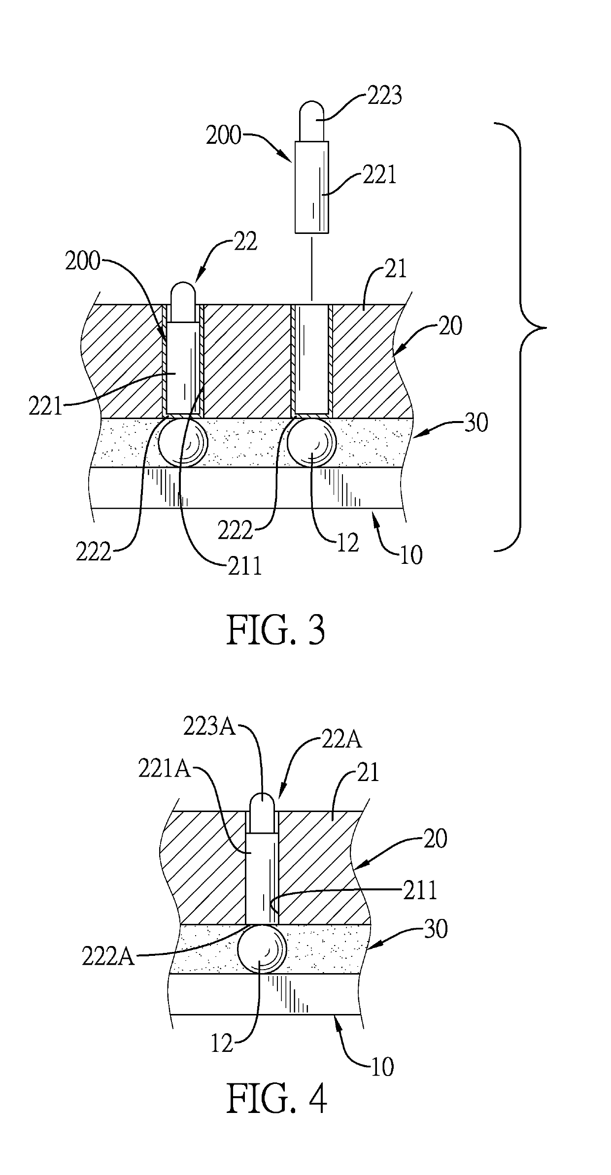
[0028]With reference to FIG. 4, in the spring probe 22A, the connecting portion 222A is formed on the top end of the base 221A. The connecting portion 222A or the base 221A is fixedly disposed in the corresponding one of the holes 211 of the plate 21 in a tight-fitting way or an adhesive bonding way.
[0029]With reference to FIG. 1, the space between the film body 11 of the film circuit board 10 and the plate 21 of the spring probe assembly 20 is filled with the filler 30 in a liquid state. The filler 30 is disposed between the film body 11 of the film circuit board 10 and the plate 21 of the spring probe assembly 20 for filling the space. Then, the filler 30 is solidified and is fixedly connected with the film circuit board 10 and the spring probe assembly 20. The film body 11 of the film circuit board 10 is supported by the filler 30. The film circuit board 10 is flat. The conductors 12 are covered by the filler 30 and then are fixed between the film body 11 and the plate 21 of the ...
PUM
 Abstract
Description
Claims
Application Information