Carrier structure and micro device structure

a micro-device and carrier technology, applied in the direction of conveyor parts, semiconductor devices, electrical equipment, etc., can solve the problems of high manufacturing cost of organic light-emitting diodes (oled) display panels, inability to compete with current mainstream displays, and inability to manufacture micro light-emitting diodes that are still more expensive to manufacture than organic light-emitting diodes, etc., to achieve good process latitude

Active Publication Date: 2019-06-20
PLAYNITRIDE DISPLAY CO LTD
View PDF0 Cites 5 Cited by
  • Summary
  • Abstract
  • Description
  • Claims
  • Application Information

AI Technical Summary

Benefits of technology

[0005]The invention provides a carrier structure with good process latitude.

Problems solved by technology

In recent years, the manufacturing cost of an organic light-emitting diode (OLED) display panel has been high and its lifetime cannot compete with current mainstream displays, and therefore a micro light-emitting diode display (micro LED display) has gradually attracted investment from various technology companies.
However, in current techniques, the micro light-emitting diode display is still more expensive to manufacture than the organic light-emitting diode display.
Although such a mass transfer technique in large-scale product manufacture has its development advantages, the current related process techniques and equipment all have bottlenecks to be broken.
In particular, the method of electrostatic force requires the use of a higher external voltage, and therefore the risk of arcing and dielectric breakdown is higher.
Therefore, more precise control is needed for the operation of the stamper, and the success rate of transfer is not high.
The transfer method involving the use of a viscous material to bond the dies has the disadvantages of uneven adhesion, instability, and poor alignment accuracy.
Moreover, when the dies are arranged on a transfer carrier via a support structure, since the support structure is mostly disposed on the peripheral surface of the dies, the dies cannot be densely arranged on the transfer carrier to efficiently perform mass transfer.
Therefore, how to solve the above technical bottlenecks and reduce production costs is one of the issues that various technology companies are currently working on.

Method used


Image

  • Carrier structure and micro device structure
  • Carrier structure and micro device structure
  • Carrier structure and micro device structure

Examples


first embodiment

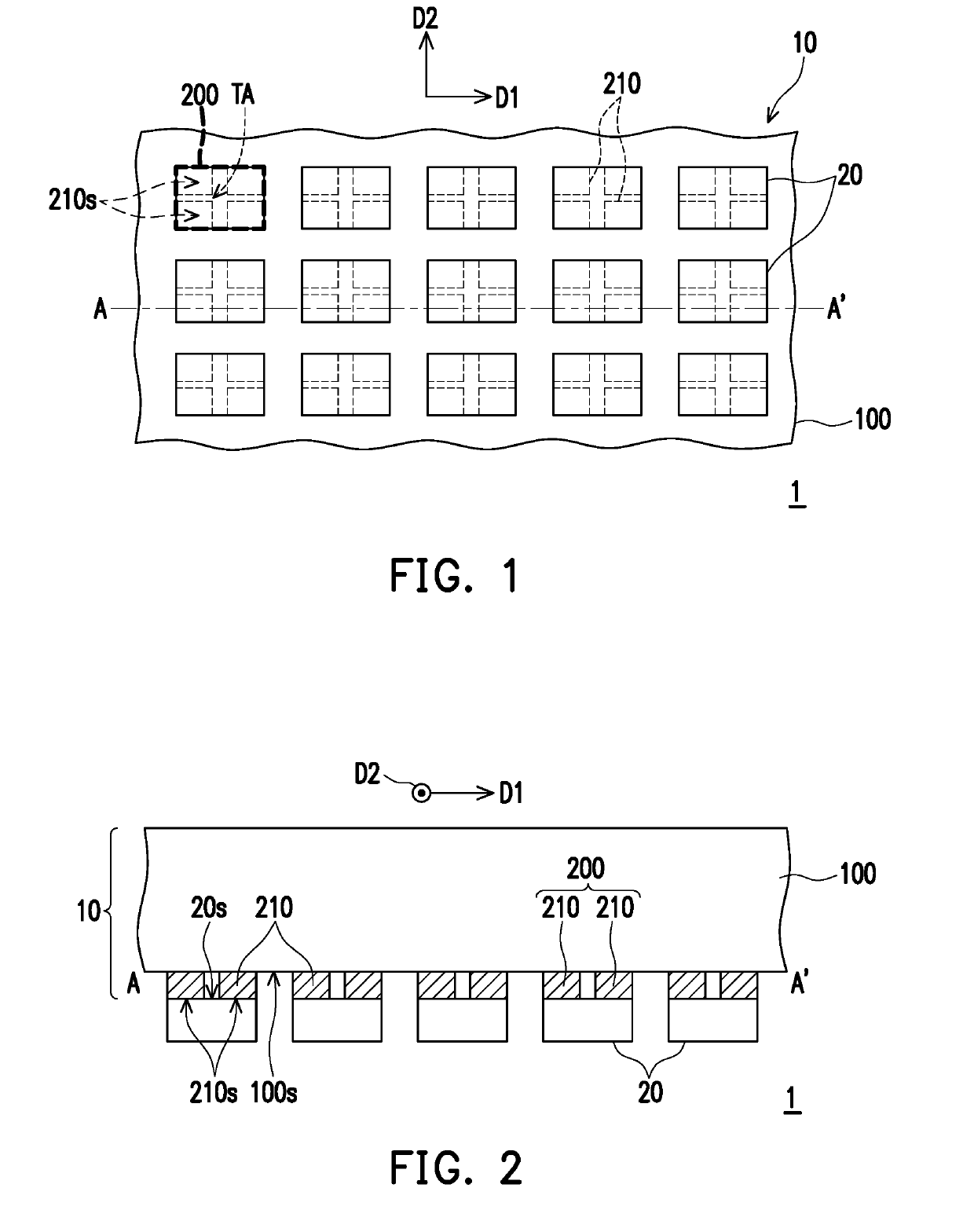
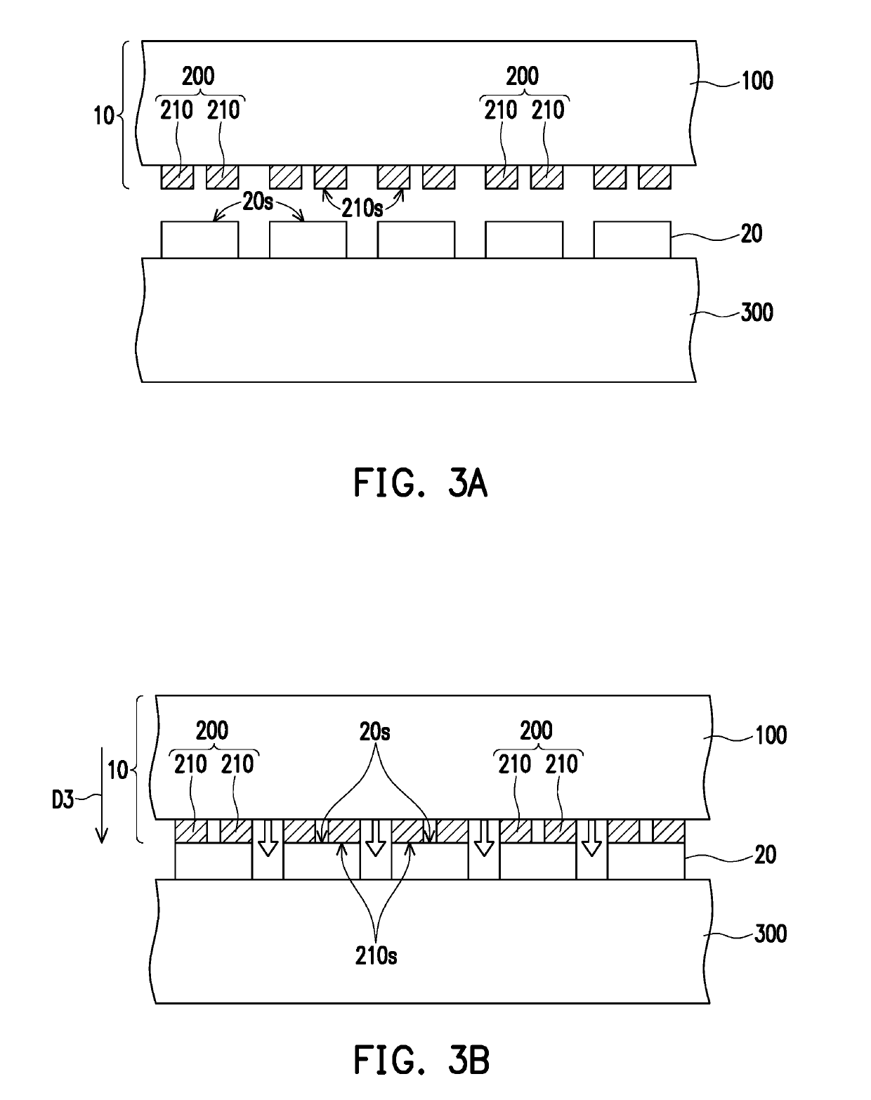
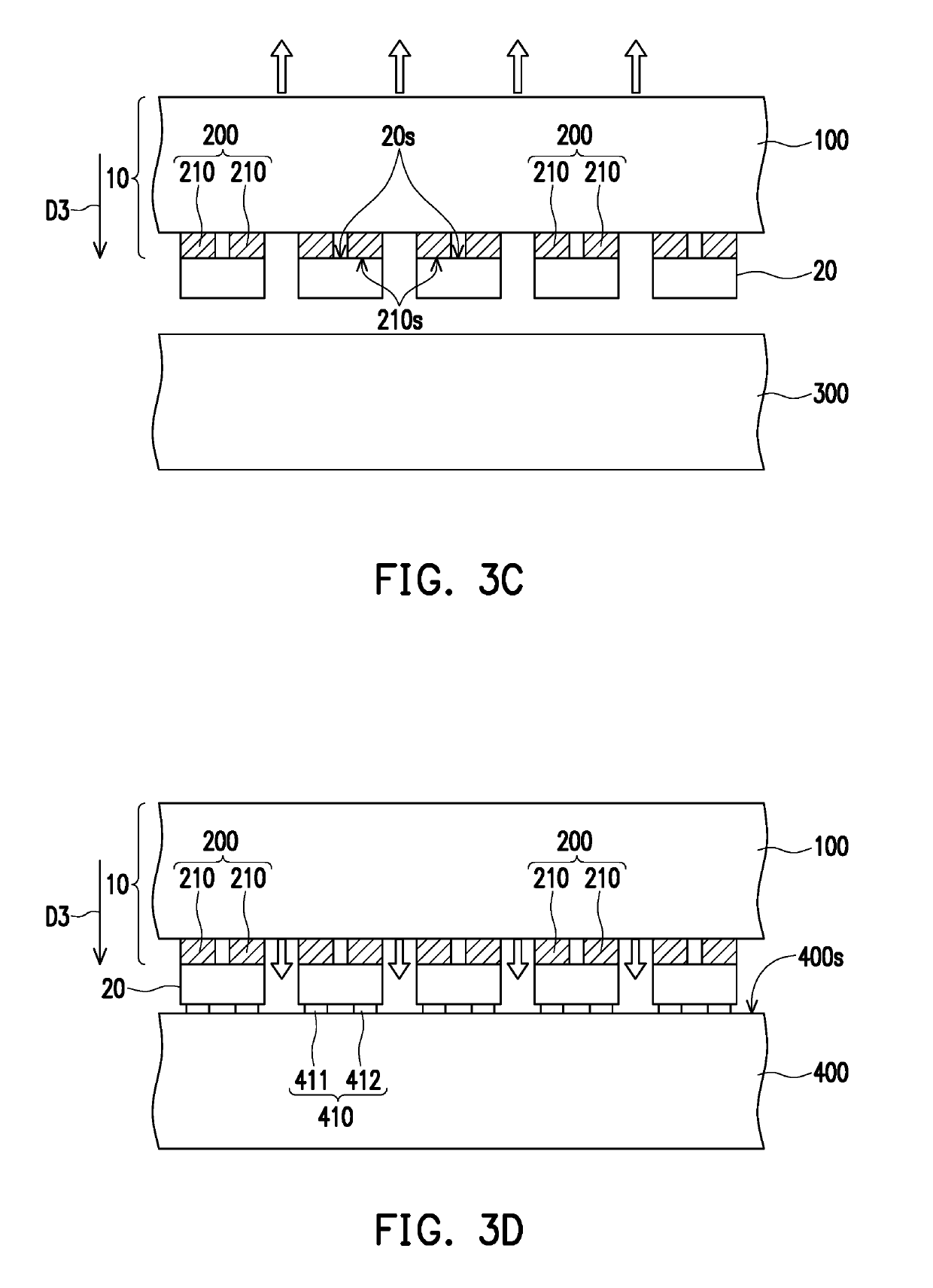
[0044]FIG. 1 is a bottom view of a micro device structure 1 of the invention. FIG. 2 is a cross section of the micro device structure 1 of FIG. 1. In particular, FIG. 2 corresponds to section line A-A′ of FIG. 1.

[0045]Referring to FIG. 1 and FIG. 2, the micro device structure 1 includes a carrier structure 10 and a plurality of micro devices 20. The carrier structure 10 is suitable for transferring the plurality of micro devices 20. The carrier structure 10 includes a carrier 100 and a plurality of transfer units 200. The plurality of transfer units 200 are disposed on the carrier 100. In detail, in the present embodiment, the plurality of transfer units 200 may be arranged in an array on a surface 100s of the carrier 100, but the invention is not limited thereto. Each of the micro devices 20 has a device surface 20s. The plurality of transfer units 200 are respectively used to connect the plurality of device surfaces 20s of the plurality of micro devices 20. Specifically, each of t...

second embodiment

[0055]FIG. 4 is a bottom view of a micro device structure 1A of the invention. FIG. 5 is a cross section of the micro device structure 1A of FIG. 4. In particular, FIG. 5 corresponds to section line B-B′ of FIG. 4.

[0056]Referring to FIG. 4 and FIG. 5, the micro device structure 1A includes a carrier structure 10A. The difference between the carrier structure 10A of the present embodiment and the carrier structure 10 of FIG. 1 is that the orthogonal projection area of the transfer region TA of each of the transfer units 200 of the carrier structure 10A of the present embodiment on the carrier 100 is greater than the area of the device surface 20s of a corresponding micro device 20A. Here, the size of the micro device 20A is, for example, less than or equal to 20 μm, and a greater misalignment latitude is required, but the invention is not limited thereto. In detail, during the transfer process of the micro device 20A, an overlapped area I of one of the transfer parts 210 of each of t...

third embodiment

[0058]FIG. 6 is a bottom view of a micro device structure 1B of the invention. FIG. 7 is a cross section of the micro device structure 1B of FIG. 6. In particular, FIG. 7 corresponds to section line C-C′ of FIG. 6.

[0059]Referring to FIG. 6 and FIG. 7, the micro device structure 1B includes a carrier structure 10B. The difference between the carrier structure 10B of the present embodiment and the carrier structure 10A of FIG. 4 is that the orthogonal projection area of the transfer region TA of each of the transfer units 200 of the carrier structure 10B of the present embodiment on the carrier 100 is less than the area of the device surface 20s of the corresponding micro device 20B. In particular, in the present embodiment, by making the ratio of the orthographic projection area of the transfer region TA of each of the transfer units 200 on the carrier 100 to the area of the device surface 20s of the corresponding micro device 20B greater than or equal to 0.5 and less than 1, the plu...


PUM


Abstract

A carrier structure suitable for transferring or supporting a plurality of micro devices including a carrier and a plurality of transfer units is provided. The transfer units are disposed on the carrier. Each of the transfer units includes a plurality of transfer parts. Each of the transfer parts has a transfer surface. Each of the micro devices has a device surface. The transfer surfaces of the transfer parts of each of the transfer units are connected to the device surface of corresponding micro device. The area of each of the transfer surfaces is smaller than the area of the device surface of the corresponding micro device. A micro device structure using the carrier structure is also provided.

Description

CROSS-REFERENCE TO RELATED APPLICATION[0001]This application claims the priority benefit of U.S. provisional application Ser. No. 62 / 607,325, filed on Dec. 19, 2017, and Taiwan application serial no. 107143613, filed on Dec. 5, 2018. The entirety of each of the above-mentioned patent applications is hereby incorporated by reference herein and made a part of this specification.BACKGROUND OF THE INVENTIONField of the Invention[0002]The invention relates to a carrier structure and a micro device structure, and more particularly, to a carrier structure suitable for transferring or supporting a micro device and a micro device structure using the carrier structure.Description of Related Art[0003]In recent years, the manufacturing cost of an organic light-emitting diode (OLED) display panel has been high and its lifetime cannot compete with current mainstream displays, and therefore a micro light-emitting diode display (micro LED display) has gradually attracted investment from various tec...

Claims


Application Information

Patent Timeline
Patent Type & Authority Applications(United States)
IPC IPC(8): H01L21/683H01L25/075B65G47/90
CPCH01L21/6835H01L25/0753B65G47/90H01L2933/0066H01L2221/68309H01L2221/68354H01L2221/68363H01L33/62H01L2221/68368
Inventor CHEN, PEI-HSINSHIH, YI-CHUNCHEN, YI-CHINGLIU, YING-TSANGLI, YU-CHUCHANG, HUAN-PUWU, CHIH-LINGLO, YU-YUNLIN, TZU-YANGLAI, YU-HUNG
Owner PLAYNITRIDE DISPLAY CO LTD
Why Eureka
Try Eureka