Check patentability & draft patents in minutes with Patsnap Eureka AI!

Linear image sensor and method for manufacturing same

a linear image sensor and photodiode technology, applied in the direction of sustainable manufacturing/processing, semiconductor/solid-state device details, radiation control devices, etc., can solve the problem of limited lengthening of linear image sensors including sensor chips having a plurality of light receiving regions (photodiodes) arranged one-dimensionally, and achieve easy to secure the flatness of the surface. , high precision

Active Publication Date: 2019-06-20
HAMAMATSU PHOTONICS KK
View PDF0 Cites 0 Cited by
  • Summary
  • Abstract
  • Description
  • Claims
  • Application Information

AI Technical Summary

Benefits of technology

The present invention is a linear image sensor that allows for precise placement of sensor chips and ensures smoothness of the sealing portion's surface.

Problems solved by technology

Lengthening of a linear image sensor including a sensor chip having a plurality of light receiving regions (photodiodes) arranged one-dimensionally is limited due to constraints of a size of a semiconductor wafer and constraints of a manufacturing apparatus, an assembling apparatus, and the like.

Method used


Image

  • Linear image sensor and method for manufacturing same
  • Linear image sensor and method for manufacturing same
  • Linear image sensor and method for manufacturing same

Examples


Embodiment Construction

[0016]Hereinafter, embodiments for carrying out the present invention will be described in detail with reference to the accompanying drawings. In the description of the drawings, the same elements will be denoted by the same reference signs, without redundant description. The present invention is not limited to these examples.

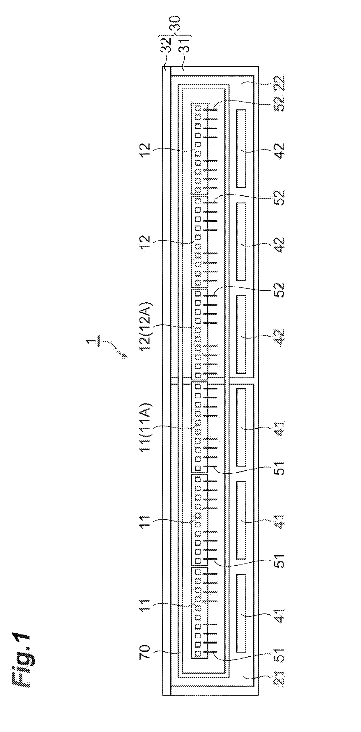
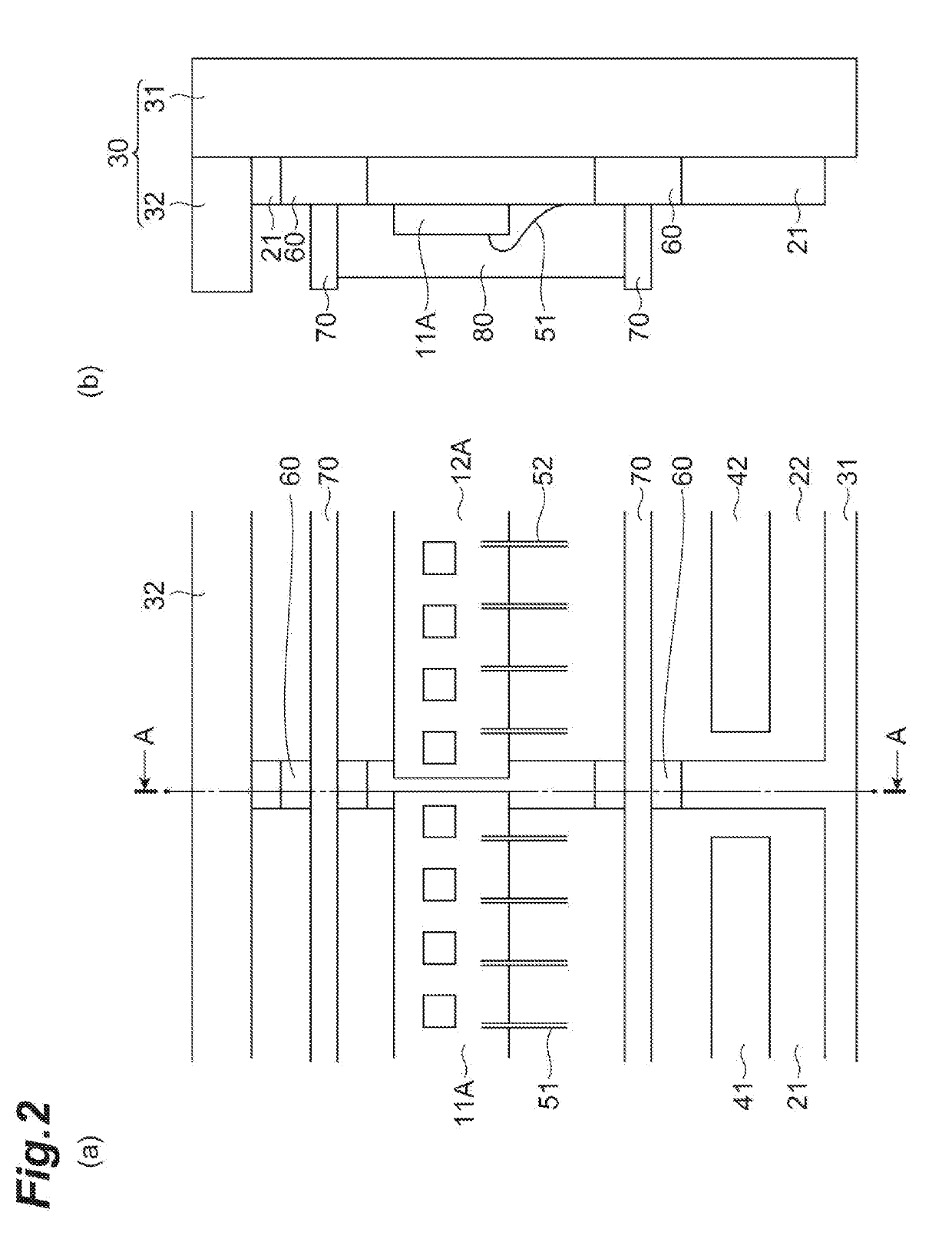
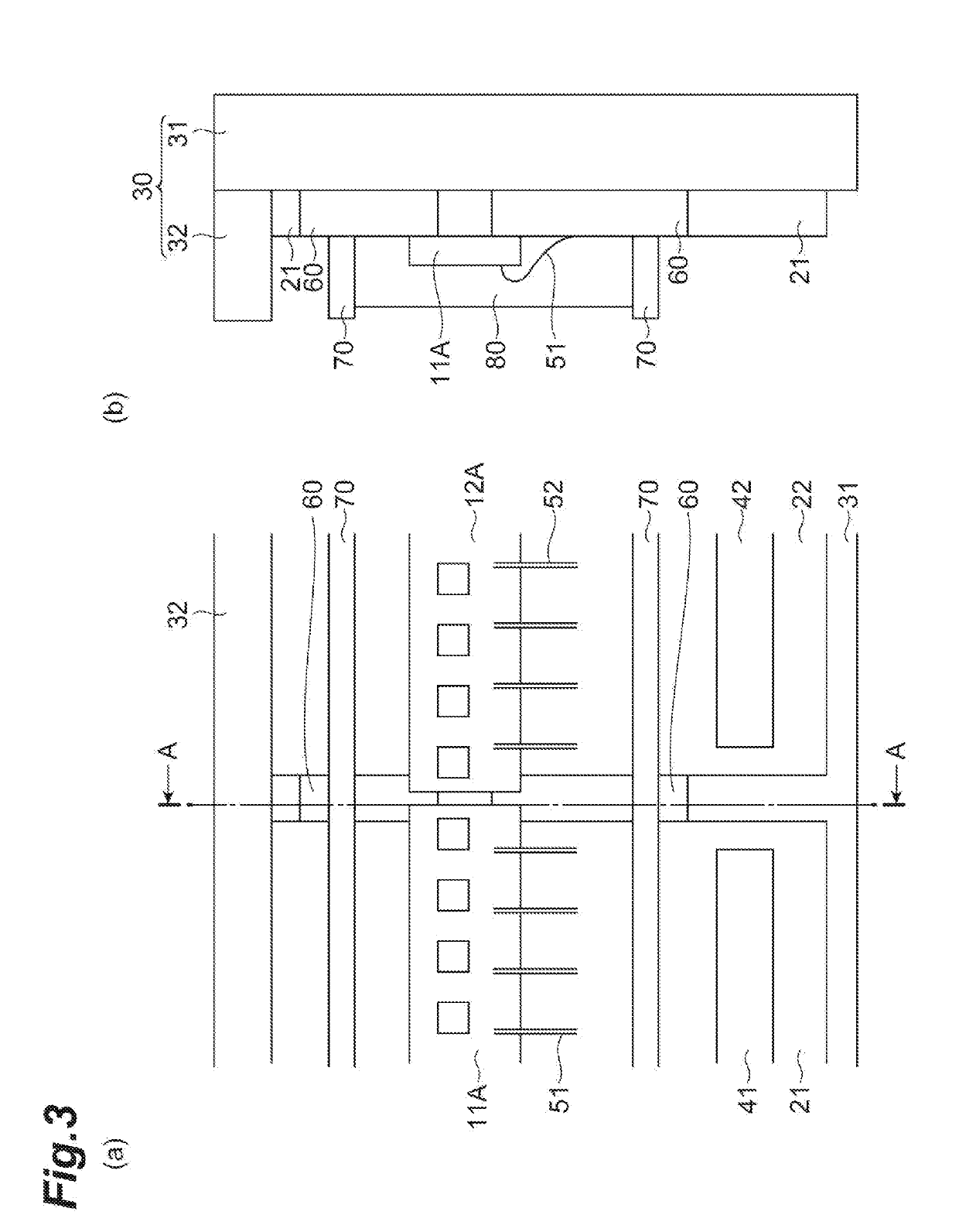
[0017]FIG. 1 is a plan view illustrating a schematic configuration of a linear image sensor 1 according to an embodiment. The linear image sensor 1 includes sensor chips 11, sensor chips 12, a first substrate 21, a second substrate 22, a common support substrate 30, connectors 41, 42, and bonding wires 51, 52, and the like.

[0018]Each of the sensor chips 11, 12 is a semiconductor chip including a plurality of light receiving regions (photodiodes) arranged at a fixed pitch in a one-dimensional form. In each of the sensor chips 11, 12, not only a light receiving region, but also a signal readout circuit that accumulates charges generated according to incidence of ...


PUM


Abstract

A linear image sensor includes first and second sensor chips, first and second substrates, a common support substrate, a support portion, a dam portion, and a sealing portion. The first sensor chip is mounted to partially protrude on one end side of the first substrate. The second sensor chip is mounted to partially protrude on one end side of the second substrate. The first and second substrates are mounted on the common support substrate. The support portion is provided in a gap between the end faces of the first and second substrates. The dam portion is provided annularly to surround the sensor chips. The sealing portion seals the sensor chips, in a region surrounded by the dam portion.

Description

TECHNICAL FIELD[0001]The present invention relates to a linear image sensor and a method for manufacturing the same.BACKGROUND ART[0002]Lengthening of a linear image sensor including a sensor chip having a plurality of light receiving regions (photodiodes) arranged one-dimensionally is limited due to constraints of a size of a semiconductor wafer and constraints of a manufacturing apparatus, an assembling apparatus, and the like. Therefore, an overall long linear image sensor is realized by disposing a plurality of sensor chips in tandem (see Patent Documents 1 and 2).CITATION LISTPatent Literature[0003]Patent Document 1: Japanese Patent Application Laid-Open Publication No. 2013-150311[0004]Patent Document 2: Japanese Patent Application Laid-Open Publication No. S64-82851SUMMARY OF INVENTIONTechnical Problem[0005]In the linear image sensor configured by disposing the plurality of sensor chips in tandem as described above, it is important that the light receiving regions are arrange...

Claims


Application Information

Patent Timeline
Patent Type & Authority Applications(United States)
IPC IPC(8): H01L27/146H01L25/04
CPCH01L27/14618H01L25/042H01L23/28H01L27/146H04N1/028Y02P70/50H01L27/14625H04N1/0318H01L2924/00014H01L2924/00H04N2201/03141H04N2201/03145H01L2224/48091H04N1/1934
Inventor MURAMATSU, NORIHIRONOZAWA, KATSUNORI
Owner HAMAMATSU PHOTONICS KK
Features
  • R&D
  • Intellectual Property
  • Life Sciences
  • Materials
  • Tech Scout
  • Unparalleled Data Quality
  • Higher Quality Content
  • 60% Fewer Hallucinations
Learn More