

Input device manufacturing method
a manufacturing method and input device technology, applied in the field of input device manufacturing methods, can solve the problems of loss of smoothness of the front surface of the input device, and achieve the effects of reducing the number of steps
- Summary
- Abstract
- Description
- Claims
- Application Information
AI Technical Summary
Benefits of technology
Problems solved by technology
Method used
Image

Examples
Embodiment Construction
[0025]An embodiment of the present invention will be described below with reference the drawings. In the descriptions below, like elements will be denoted by like reference characters and repeated descriptions will be appropriately omitted for members that have been described once.
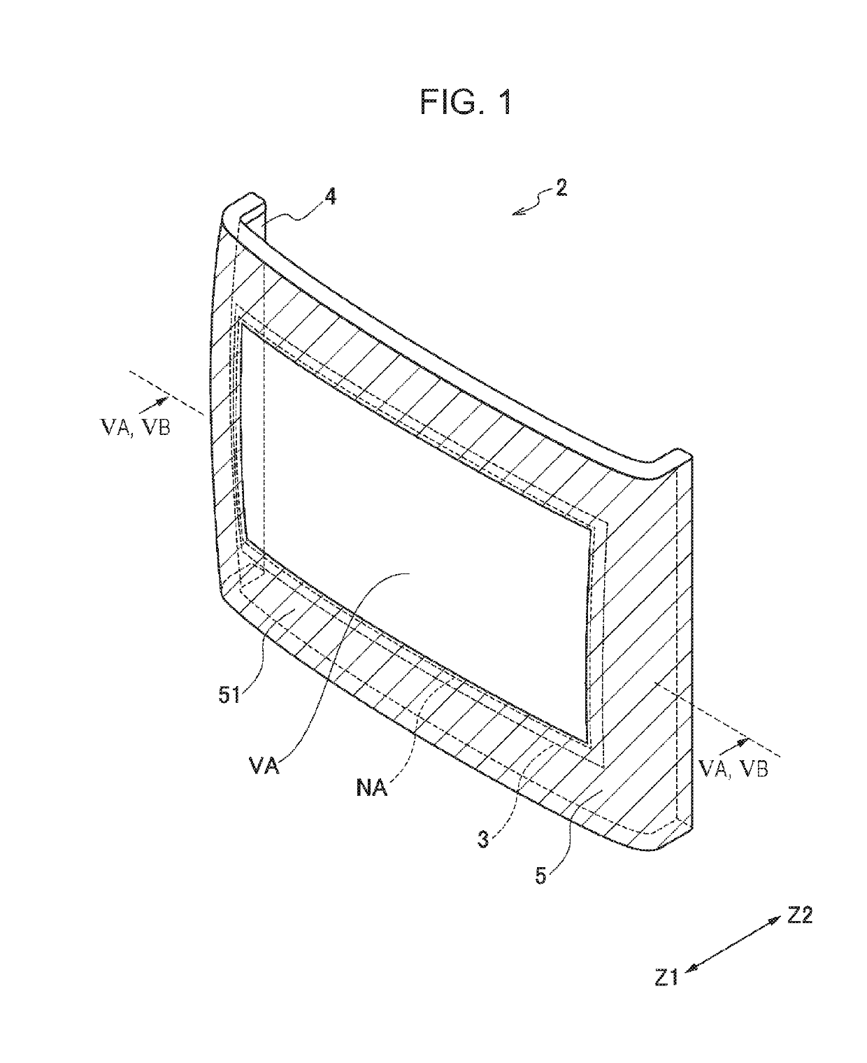
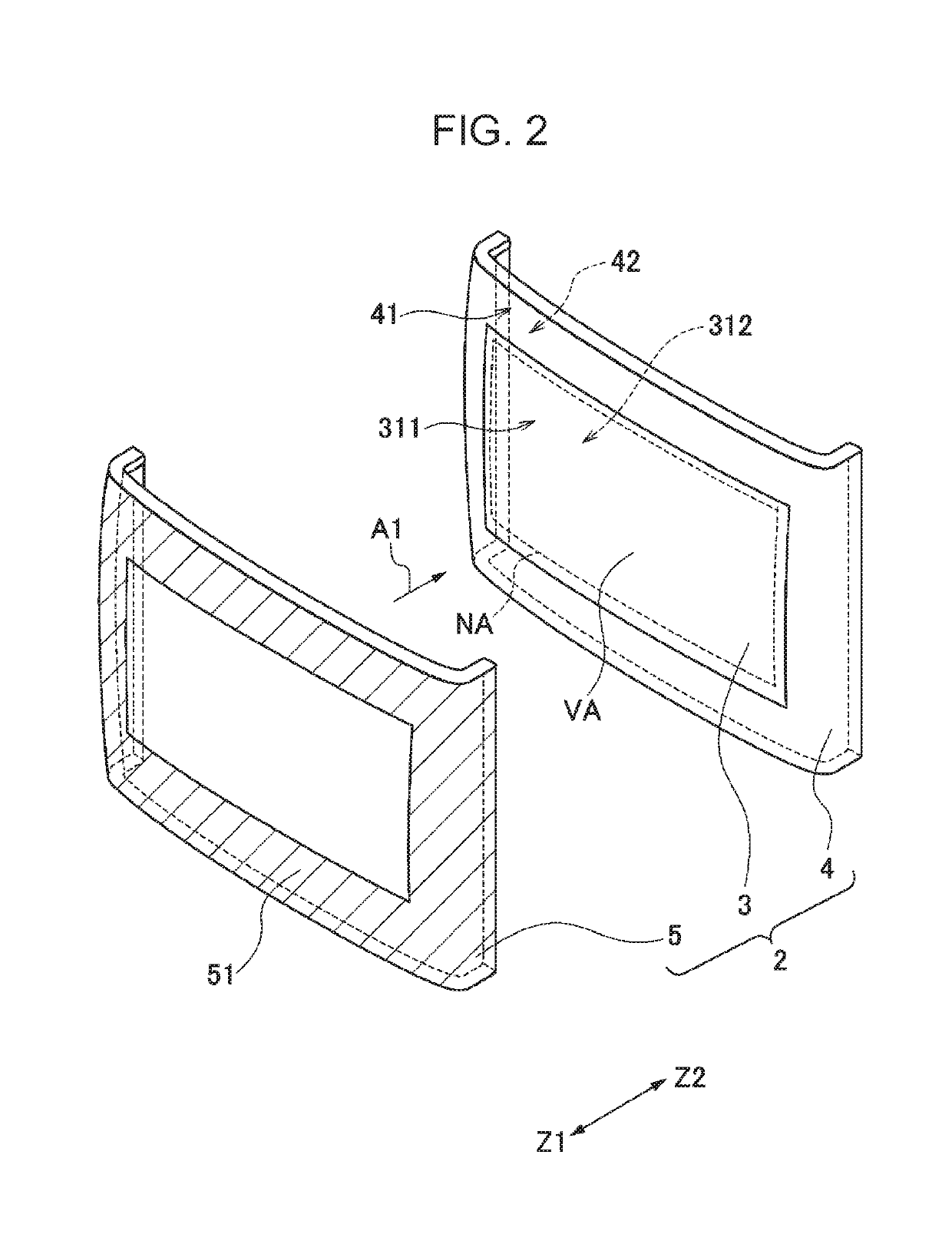
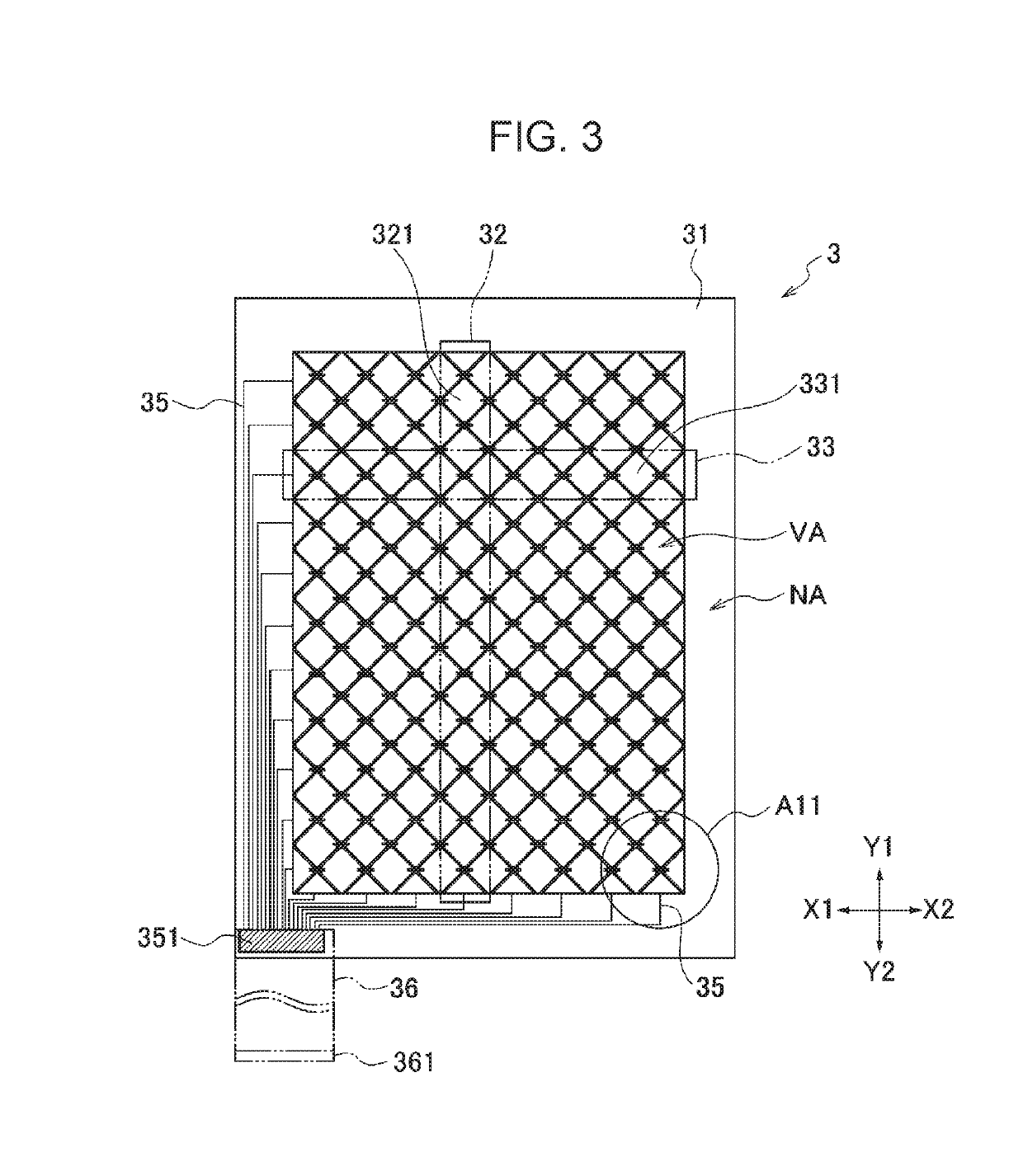
[0026]FIG. 1 is a perspective view illustrating an input device manufactured by a manufacturing method according to an embodiment of the present invention. FIG. 2 is an exploded view illustrating the input device manufactured by the manufacturing method according to the embodiment of the present invention. FIG. 3 is a plan view illustrating a sensor film in the embodiment of the present invention. FIG. 4 is an enlarged view in which the area A11 indicated in FIG. 3 is enlarged.
[0027]Before an input device manufacturing method according to this embodiment will be described, the input device manufactured by the manufacturing method will be described first. In the specification of this application, “transpare...
PUM
 Abstract
Description
Claims
Application Information