Method of and system for performing defect detection on or characterization of a layer of a semiconductor element or semi-manufactured semiconductor element

a technology of semiconductor elements and defects, applied in semiconductor/solid-state device testing/measurement, scanning probe techniques, instruments, etc., can solve the problems of prone to defects in self-assembled monolayers or directed self-assembled layers, affecting the quality of semiconductor components, and causing defects of at least this size to be created. time efficient and accurate

Active Publication Date: 2019-07-25
NEDERLANDSE ORG VOOR TOEGEPAST-NATUURWETENSCHAPPELIJK ONDERZOEK (TNO)
View PDF0 Cites 0 Cited by
  • Summary
  • Abstract
  • Description
  • Claims
  • Application Information

AI Technical Summary

Benefits of technology

[0005]It is an object of the present invention to provide method of performing defect detection on or characterization of a self-assembled monolayer or a directed self-assembled layer of a semiconductor element or semi-manufactured semiconductor element, which method is time efficient and accurate such as to be suitable for application in a manufacturing process.

Problems solved by technology

With the ongoing miniaturization of semiconductor elements to achieve even faster chips, higher processing capability, and broader fields of application, the manufacturing thereof becomes more an more challenging.
Although the above technique works very well in creating ingenious two dimensional and three dimensional semiconductor device structures of very small dimensions (below 20 nanometer), the technology is prone to defects in the self-assembled monolayer or directed self-assembled layer.
If a single molecule is missing, this will create a defect of at least this size.
Directed self-assembled layers are likewise fragile and prone to missing molecules that may interfere with their application, e.g. in a patterning process.

Method used


Image

  • Method of and system for performing defect detection on or characterization of a layer of a semiconductor element or semi-manufactured semiconductor element
  • Method of and system for performing defect detection on or characterization of a layer of a semiconductor element or semi-manufactured semiconductor element
  • Method of and system for performing defect detection on or characterization of a layer of a semiconductor element or semi-manufactured semiconductor element

Examples


Embodiment Construction

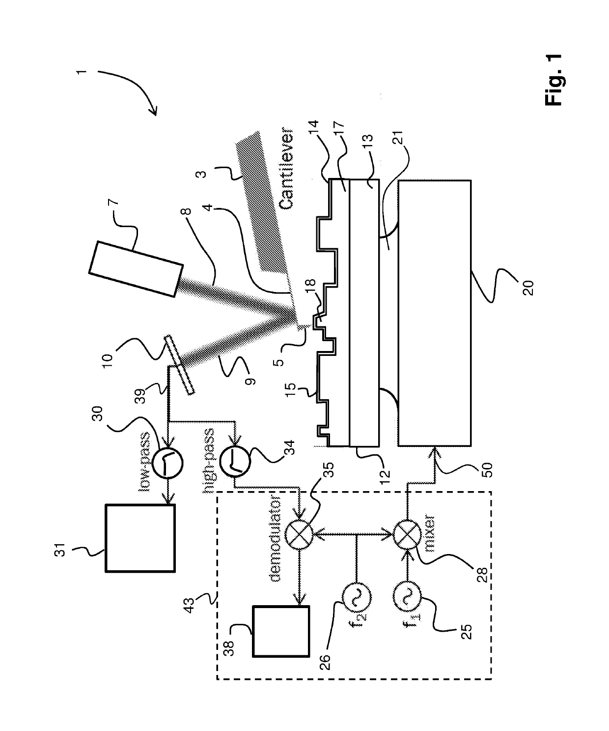
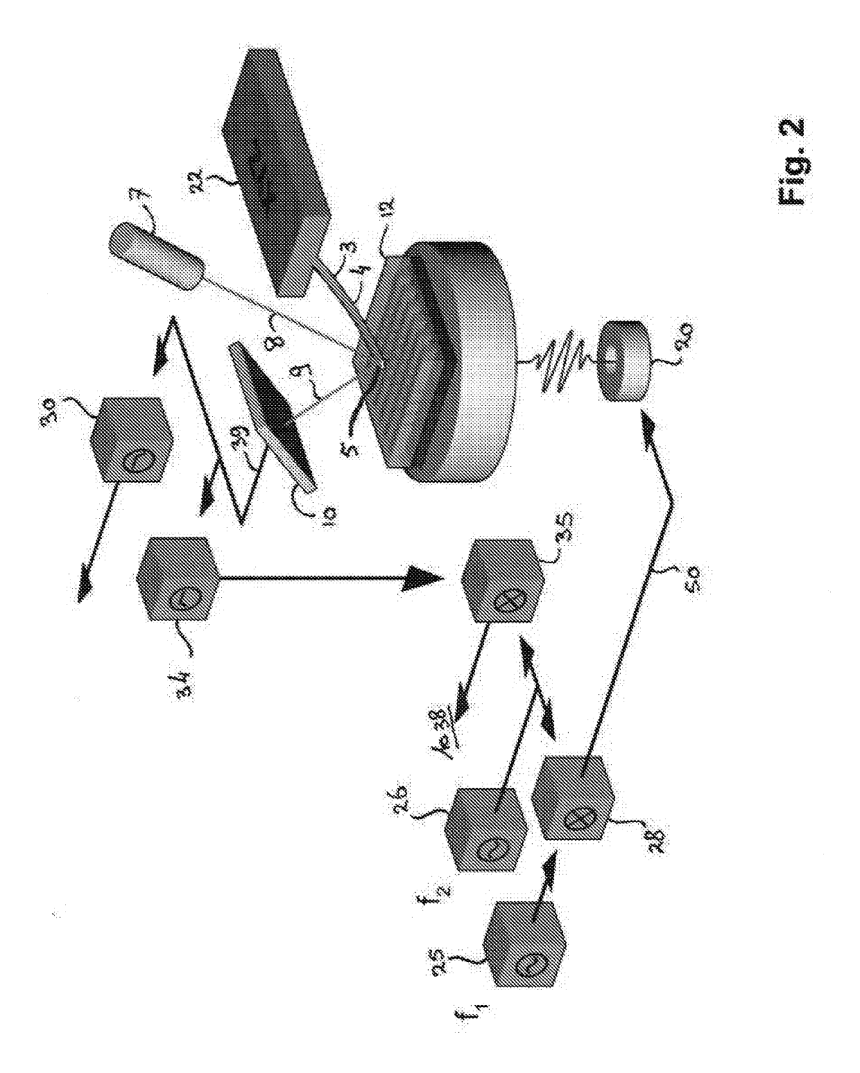
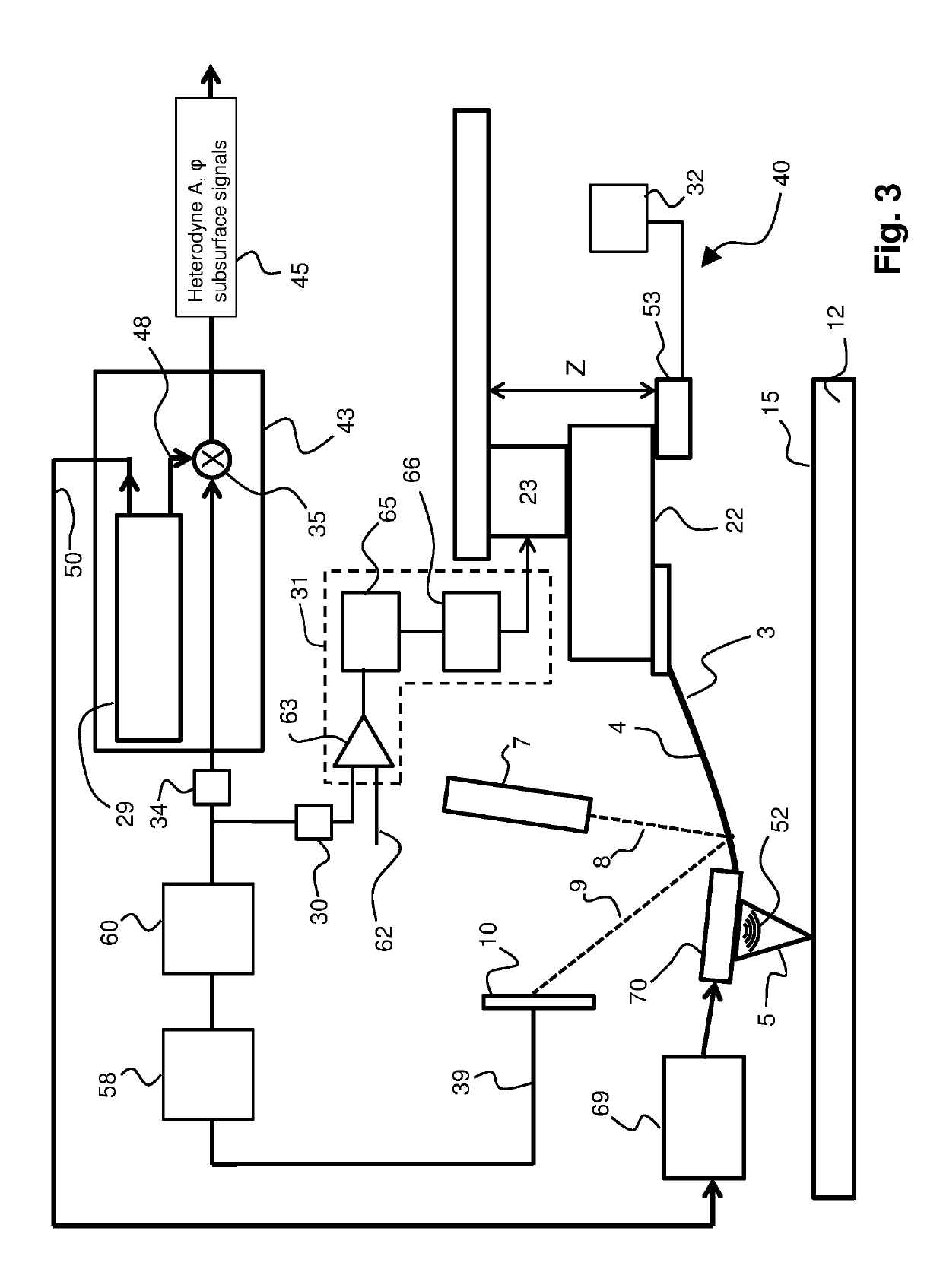
[0024]FIG. 1 schematically illustrates an atomic force microscopy system (AFM) 1, suitable for use in a method of the present invention and in accordance with an embodiment of the present invention. Another impression of the system 1 of FIG. 1 is illustrated in FIG. 2, reciting corresponding reference numerals. The system 1 comprises a probe 3 having a cantilever 4 and a probe tip 5. The probe tip 5 is brought in contact with a surface 15 of a self-assembled monolayer 14 on a semi-manufactured semiconductor element 12. A light source 7, typically a laser, provides an optical signal beam 8 that is incident on the back of the probe tip 5. A reflected optical beam 9 is received by an optical sensor 10. Any vibration of the probe tip 5 perpendicular to the surface 15 of the monolayer 14 will result in a deflection of the reflected optical beam 9. This deflection can be accurately determined by means of optical sensor 10 which provides an (electrical) output signal 39 for further analysi...


PUM

PropertyMeasurementUnit
sizeaaaaaaaaaa
sizeaaaaaaaaaa
modulation frequencyaaaaaaaaaa

Abstract

The present document relates to a method of performing defect detection on a self-assembled monolayer of a semiconductor element or semi-manufactured semiconductor element, using an atomic force microscopy system. The system comprises a probe with a probe tip, and is configured for positioning the probe tip relative to the element for enabling contact between the probe tip and a surface of the element. The system comprises a sensor providing an output signal indicative of a position of the probe tip. The method comprises: scanning the surface with the probe tip; applying an acoustic vibration signal to the element; obtaining the output signal indicative of the position of the probe tip; monitoring probe tip motion during said scanning for mapping the surface of the semiconductor element, and using a fraction of the output signal for mapping contact stiffness indicative of a binding strength.

Description

FIELD OF THE INVENTION[0001]The present invention is directed at a method of performing defect detection on or characterization of a layer of a semiconductor element or semi-manufactured semiconductor element, the layer being a self-assembled monolayer or a directed self-assembled layer. The invention is further directed at a method of manufacturing a semiconductor element or semi-manufactured semiconductor element, and at an atomic force microscopy system.BACKGROUND[0002]With the ongoing miniaturization of semiconductor elements to achieve even faster chips, higher processing capability, and broader fields of application, the manufacturing thereof becomes more an more challenging. Conventional manufacturing methods such as lithographic methods are approaching the boundaries of what is achievable in view of the desired dimensions. Therefore, other technologies are being explored that enable to further decrease the scale of dimensions at which semiconductor elements may be manufactur...

Claims


Application Information

Patent Timeline
Patent Type & Authority Applications(United States)
IPC IPC(8): G01Q20/00G01N29/06G01N29/04H01L21/66
CPCG01Q20/00G01N29/0681G01N29/041H01L22/12G01N2291/2697G01Q60/32G01N2291/0427H01L22/24G01N29/00
Inventor SADEGHIAN MARNANI, HAMEDVAN ES, MAARTEN HUBERTUSMEIJER TIMMERMAN THIJSSEN, RUTGER
Owner NEDERLANDSE ORG VOOR TOEGEPAST-NATUURWETENSCHAPPELIJK ONDERZOEK (TNO)
Why Eureka
Try Eureka