

Semiconductor device
- Summary
- Abstract
- Description
- Claims
- Application Information
AI Technical Summary
Benefits of technology
Problems solved by technology
Method used
Image



Examples
first embodiment
[0022]FIG. 1 is a conceptual view of a semiconductor device according to the present invention.
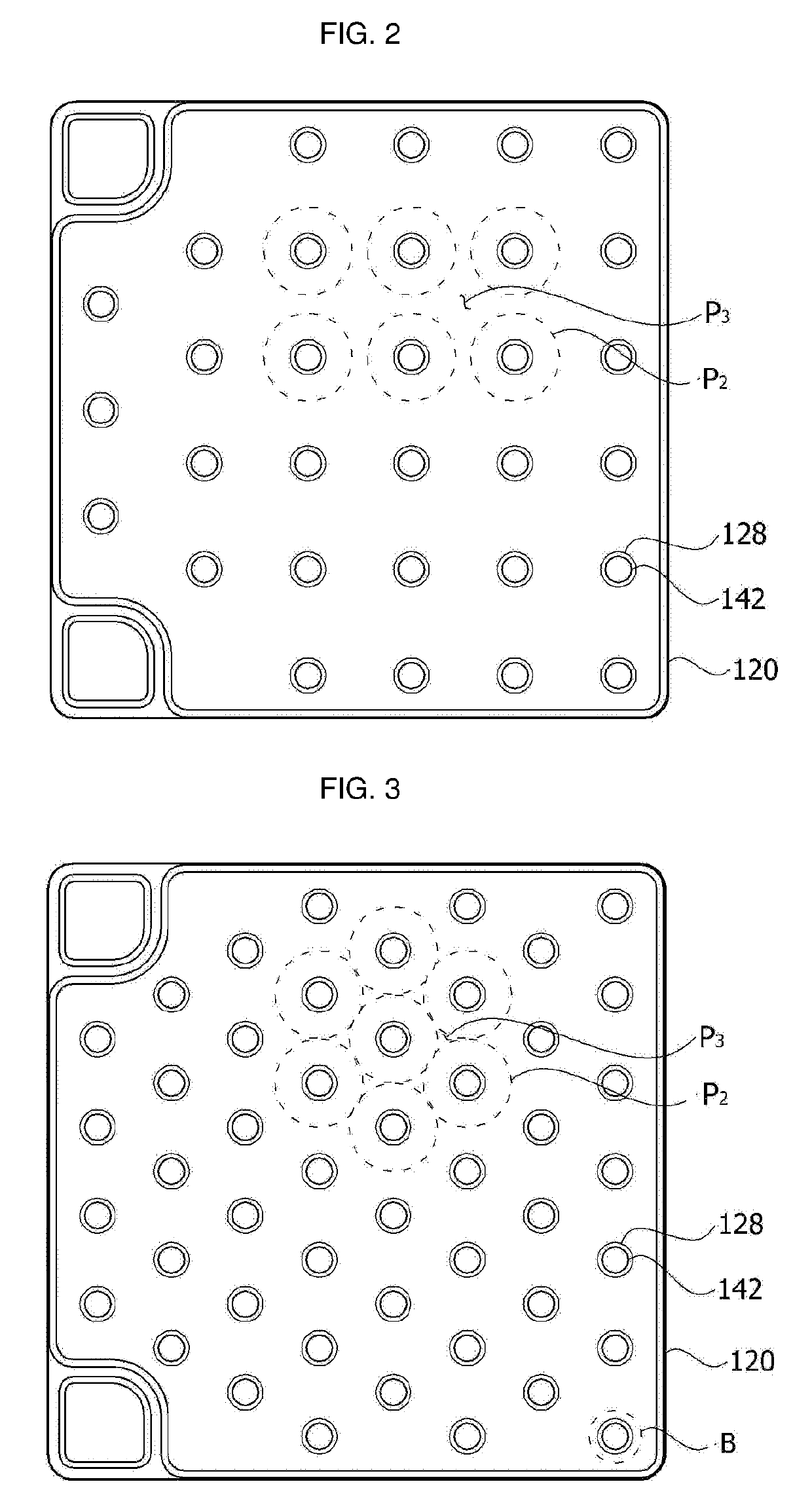
[0023]FIGS. 2 and 3 are views illustrating a configuration in which optical output power is enhanced depending on a change in number of recesses.
[0024]FIG. 4 is an enlarged view of a part A of FIG. 1.
[0025]FIG. 5 is an enlarged view of a part B of FIG. 3.
[0026]FIG. 6 is an enlarged view of a part C of FIG. 4.
[0027]FIG. 7 is a diagram showing a layer structure of a first electrode and a reflective layer.
[0028]FIG. 8A is a first modification of FIG. 6.
[0029]FIG. 8B is a second modification of FIG. 6.
[0030]FIG. 9 is a third modification of FIG. 6.
[0031]FIG. 10 is a diagram showing various shapes of a reflective layer.
second embodiment
[0032]FIG. 11 is a conceptual view of a semiconductor device according to the present invention.
third embodiment
[0033]FIG. 12 is a sectional view of a semiconductor device according to the present invention.
[0034]FIG. 13A is an enlarged view of a part A of FIG. 12.
[0035]FIG. 13B is a modification of FIG. 13A.
[0036]FIG. 14A is a plan view of the semiconductor device according to the third embodiment of the present invention.
[0037]FIG. 14B is a plan view showing an etching region of a first electrode according to the third embodiment of the present invention.
[0038]FIG. 14C is a modification of FIG. 14B.
[0039]FIG. 14D is a plan view showing a first cover electrode and a second cover electrode according to the third embodiment of the present invention.
[0040]FIG. 14E is a modification of FIG. 14D.
[0041]FIGS. 15A and 15B are a plan view and a sectional view in which a light emitting region is formed through mesa etching.
[0042]FIGS. 16A and 16B are a plan view and a sectional view in which a first electrode is formed.
[0043]FIGS. 17A and 17B are a plan view and a sectional view in which a second elec...
PUM
 Abstract
Description
Claims
Application Information