Power electronics module and a method of producing a power electronics module

a technology of power electronics and electronics modules, applied in the direction of printed circuit assembling, printed circuit manufacturing, semiconductor/solid-state device details, etc., to achieve the effects of low thermal resistivity, reliable heat transfer structure, and enhanced heat transfer

Active Publication Date: 2019-08-01
ABB (SCHWEIZ) AG
View PDF26 Cites 2 Cited by
  • Summary
  • Abstract
  • Description
  • Claims
  • Application Information

AI Technical Summary

Benefits of technology

[0014]The invention is based on the idea forming the base plate of a power electronics module from a soft material such that the base plate is compressible. When attached to a cooling device, the base plate deforms and produces a reliable heat transfer structure from the substrate to the cooling device. When the base plate deforms, it fills all possible gaps that are in the surface of the cooling device and thereby provides low thermal resistivity and enhances the heat transfer. Further, as the base plate is compressible, the substrate “floats” inside the power electronics module on top of the base plate. Possible mechanical forces acting on the module are dampened and do not reach the substrate as easily as in known modules.
[0015]As the base plate of the power electronics module of the invention is soft and compressible, separate thermal interface material layers between the base plate and the cooling element can be avoided. The avoidance of separate material layers which are to be applied during installation of the module help in decreasing the thermal resistivity between the heat sources, i.e. semiconductor chips, and the cooling element. This further means that the heat transfer capacity is increased.
[0016]The installation of the module of the invention is further simple, as thermal interface material layers are not required between the base plate and the cooling element.
[0017]The installation with the interface layers is cumbersome as the layers are very thin and brittle or fold easily during installation. With the module of the present invention, the cooling element, such as a heat sink, can be attached directly to the base plate of the module without any intermediate layers. During use, the thermal interface material layers can also break which leads to increased chip temperatures.

Problems solved by technology

Possible mechanical forces acting on the module are dampened and do not reach the substrate as easily as in known modules.

Method used


Image

  • Power electronics module and a method of producing a power electronics module
  • Power electronics module and a method of producing a power electronics module
  • Power electronics module and a method of producing a power electronics module

Examples


Embodiment Construction

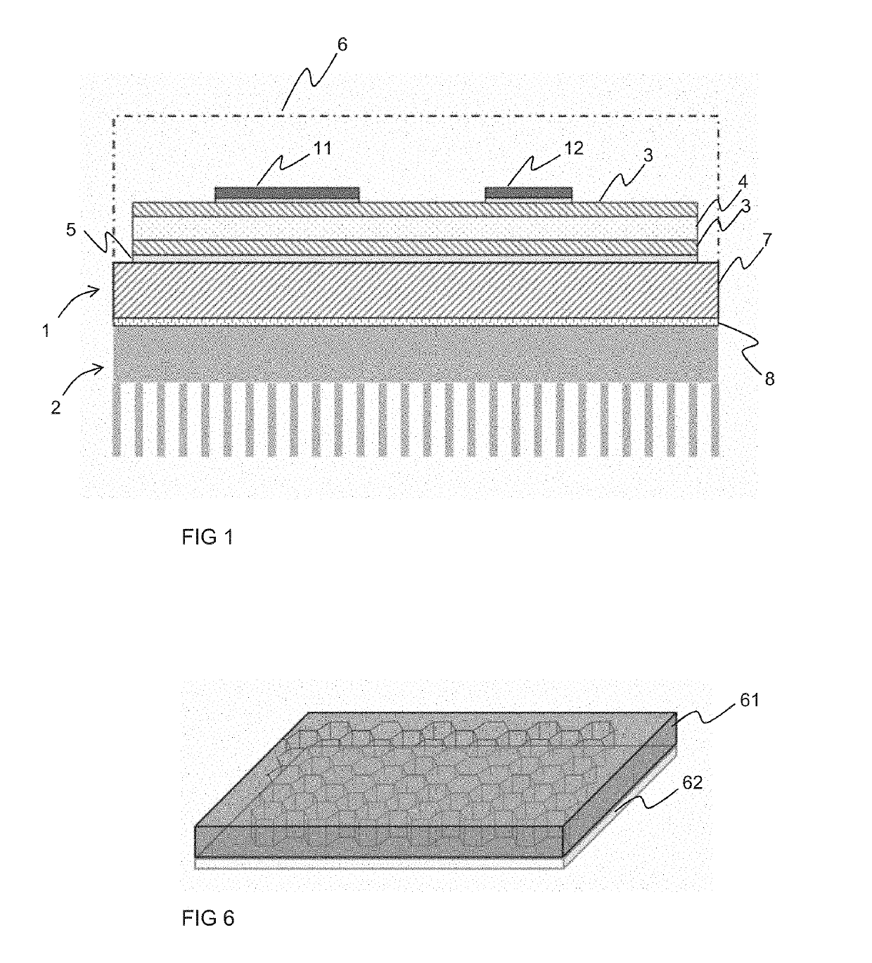
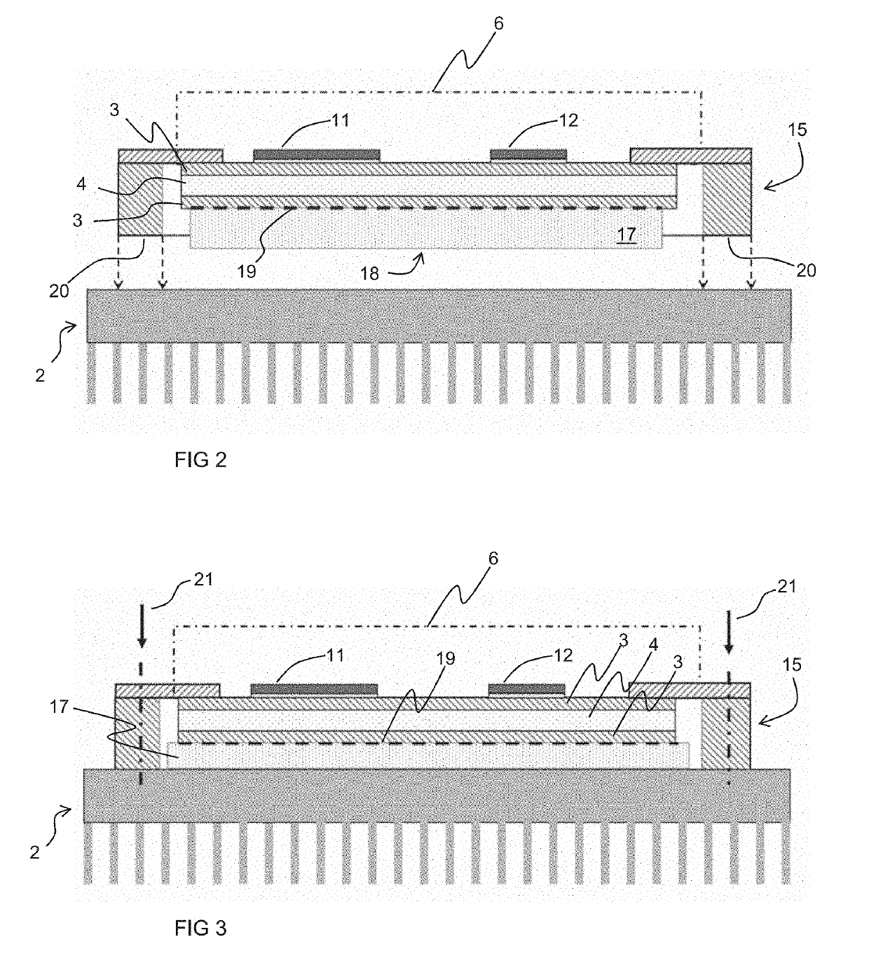
[0024]FIG. 2 shows a cross section of a power electronics module according to an embodiment of the present invention. The cross section of FIG. 2 shows power semiconductor chips 11, 12 soldered to a substrate, such as DBC structure 3, 4. According to the present invention, the power electronics module comprises multiple of power electronic semiconductor chips incorporated in a housing and attached to a substrate. In the description and drawings reference is made specifically to direct bonded copper structure as an example of the substrate. The cross section of FIG. 2 shows only two semiconductor chips 11, 12. However, the number of the chips is not limited to any particular number.

[0025]The power electronics module further comprises a heat transfer structure attached to the substrate and having a bottom surface which forms an outer surface of the module and which is adapted to receive a surface of a cooling device. As known, the heat from the semiconductor chips is typically removed...


PUM


Abstract

A power electronics module and a method of producing a power electronics module. The power electronics module includes multiple of power electronic semiconductor chips incorporated in a housing and attached to a substrate, and a heat transfer structure attached to the substrate and having a bottom surface which forms an outer surface of the module and which is adapted to receive a surface of a cooling device, wherein the heat transfer structure includes a compressible base plate.

Description

FIELD OF THE INVENTION[0001]The invention relates to power electronics modules, and particularly to a power electronics module with improved cooling properties.BACKGROUND OF THE INVENTION[0002]Power electronics modules are commonly used in high powered devices for switching high currents and operating on high voltages. Power electronics modules contain multiple of switch components which are situated in a same component housing and typically internally connected to each other to provide a certain circuit structure.[0003]Power electronics modules are used, for example, for producing certain power conversion circuits, such as inverters and converters. An example of a power electronics module contains two IGBTs (Insulated Gate Bi-polar Transistors) which are connected in series inside the module. Other examples may include bridge topologies or parts of bridge topologies which are readily electrically connected inside the module.[0004]Power electronics modules may also comprise a base p...

Claims


Application Information

Patent Timeline
Patent Type & Authority Applications(United States)
IPC IPC(8): H05K1/02H05K3/00H05K3/34H01L23/373
CPCH05K1/0203H05K3/0061H05K3/341H01L23/3735H01L23/14H01L23/373H01L23/42H01L23/433
Inventor MANNINEN, JORMASILVENNOINEN, MIKAPAKARINEN, JONIINGMAN, KJELL
Owner ABB (SCHWEIZ) AG
Why Eureka
Try Eureka