Contact sensitive device, display apparatus including the same and method of manufacturing the same

a technology of contact sensitive devices and display devices, which is applied in the direction of mechanical pattern conversion, graph reading, instruments, etc., can solve the problems of difficult modulation frequency, difficulty in providing immediate and minute feedback in response to the touch of the user, and large size of such devices to increase the intensity of vibration, so as to improve piezoelectricity and light transmittance of contact sensitive devices. , the effect of improving piezoelectricity

Active Publication Date: 2019-08-15
LG DISPLAY CO LTD
View PDF6 Cites 0 Cited by
  • Summary
  • Abstract
  • Description
  • Claims
  • Application Information

AI Technical Summary

Benefits of technology

[0007]Another exemplary objective of the present disclosure is to provide a contact sensitive device having improved driving displacement and vibration intensity, a display apparatus including the same, and a method of manufacturing the same.
[0025]According to the present disclosure, a contact sensitive device including an electroactive layer with improved piezoelectricity may be provided, because the electroactive layer may have a β-phase without performing a stretching process or a polling process. Further, piezoelectricity and light transmittance of the contact sensitive device may be improved.

Problems solved by technology

Thus, it is difficult to provide immediate and minute feedback in response to the touch of the user.
However, the size of such devices needs to be increased to increase the intensity of the vibrations, because the vibration motor is configured to vibrate the entire display apparatus.
Further, is difficult to modulate a frequency of the vibration motor to adjust the level of the vibrations, and a response speed is very low, which are problematic.
Furthermore, the eccentric rotating mass and the linear resonant actuator are formed of opaque materials, and thus, it is difficult to dispose the eccentric rotating mass and the linear resonant actuator above the display panel.
However, the shape memory alloy (SMA) has a low response speed, a short life-span, and is formed of an opaque material.
On the other hand, electro-active ceramics (EAC) have low durability against the external impact, and are easily broken due to external impact.
Further, it is difficult to manufacture a thin electro-active ceramic.

Method used


Image

  • Contact sensitive device, display apparatus including the same and method of manufacturing the same
  • Contact sensitive device, display apparatus including the same and method of manufacturing the same
  • Contact sensitive device, display apparatus including the same and method of manufacturing the same

Examples


example 3

Preparative Preparation of PS-PVDF-PS Block Copolymer

[0110]The chlorine terminated PVDF prepared in Preparative Example 2 and styrene were polymerized for five hours at 110° C. at a volume fraction of 6:4. Thereafter, the PS-PVDF-PS block copolymer was crystalized from the reaction mixture and dried.

example 1

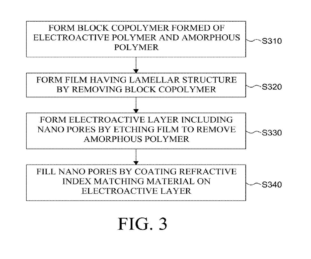
[0111]10 weight % of the PS-PVDF-PS block copolymer (PVDF:PS=6:4 in volume fraction) prepared in Preparative Examples 1 to 3 was dissolved in DMF. The prepared solution was spin-coated and then dried for 30 minutes at 120° C. to prepare a PS-PVDF-PS block copolymer film having a lamellar structure. Thereafter, the prepared block copolymer film was dipped in 98% of a nitrate solution for five minutes to remove polystyrene via an etching process, and an electroactive layer having a thickness of 10 μm and a plurality of nano pores was formed. Thereafter, PVDF-TRFF-CFE terpolymer serving as a refractive index matching material was coated on the electroactive layer to form an electroactive layer having a final thickness of 35 μm.

experimental example 1

ty of Electroactive Layer

[0114]A cross-section of the electroactive layer prepared according to Example 1 was imaged using an SEM at a magnification of 50000. The SEM image is shown in FIG. 5.

[0115]As shown in FIG. 5, nano pores x are formed on the electroactive layer in Example 1 and the nano pores x and the PVDF-based polymer y are arranged in the same direction. That is, a lamellar structure is formed. Further, the pore diameter in a thickness direction of the nano pores x is approximately 50 nm to 100 nm and the distance between nano pores x is approximately 20 nm to 100 nm.


PUM

PropertyMeasurementUnit
refractive indexaaaaaaaaaa
densityaaaaaaaaaa
porosityaaaaaaaaaa

Abstract

Provided are a contact sensitive device, a display apparatus including the same, and a method of manufacturing the same. The contact sensitive device includes an electroactive layer formed of an electroactive polymer having a plurality of nano pores and an electrode disposed on at least one surface of the electroactive layer. The electroactive layer has a β-phase structure and improved piezoelectricity without performing a stretching process or a polling process.

Description

CROSS-REFERENCE TO RELATED APPLICATIONS[0001]This application claims priority from Korean Patent Application No. 10-2015-0191610 filed on Dec. 31, 2015, the disclosure of which is incorporated by reference in its entirety as if fully set forth herein.BACKGROUNDTechnical Field[0002]The present disclosure relates to a contact sensitive device, a display apparatus including the same, and a method of manufacturing the same, including a contact sensitive device which includes an electroactive layer formed of an electroactive polymer, a display apparatus including the same, and a method of manufacturing the same.Description of the Related Art[0003]Recently, a touch type display apparatus which inputs information by touching a display apparatus is in common use because of an increase in demand for such devices from users using various display apparatus, including liquid crystal display devices and organic light emitting display devices. In response to this, there is ongoing study related t...

Claims


Application Information

Patent Timeline
Patent Type & Authority Applications(United States)
IPC IPC(8): G06F3/041H01L41/047G06F3/01H01L41/09H01L41/253H01L41/193H01L41/113H01L41/45
CPCG06F3/0416H01L41/0477G06F3/016G06F3/041H01L41/09H01L41/253H01L41/193H01L41/1132H01L41/45G06F2203/04103C08J9/26C08J2201/0464C08J2353/00G06F3/0412H10N30/857H10N30/206H10N30/20H10N30/302H10N30/852H10N30/092H10N30/04H10N30/098H10N30/877
Inventor CHOI, SEULGIHAM, YONG-SUKIM, TAEHEONLEE, YONGWOOKHO, YUSEONLIM, MYUNGJIN
Owner LG DISPLAY CO LTD
Why Eureka
Try Eureka