Semiconductor device including clock generation circuit

a technology of clock generation circuit and semiconductor device, which is applied in the direction of generating/distributing signals, pulse techniques, instruments, etc., can solve the problems of not being able to perform a test appropriate, the operation speed of the tester used for testing the semiconductor device may not keep up with the increase, and the test may take a long tim

Active Publication Date: 2019-08-29
SK HYNIX INC
View PDF4 Cites 0 Cited by
  • Summary
  • Abstract
  • Description
  • Claims
  • Application Information

AI Technical Summary

Benefits of technology

[0009]In accordance with an embodiment of the present invention, a clock generation circuit includes: a frequency detector suitable for generating an internal clock, and generating a counting signal indicating a toggling number of the internal clock during an activation period of an input clock; a control signal generator suitable for generating a plurality of period control signals based on a target signal and the counting signal, the target signal indicating a target frequency of an output clock; and a period controller suitable for generating the output clock based on the period control signals.
[0010]In accordance with another embodiment of the present invention, a semiconductor system includes: a test apparatus suitable for providing a semiconductor device with a reference clock; and a semiconductor device suitable for receiving the reference clock and generating an output clock for an operation of the semiconductor device, wherein the semiconductor device includes: a frequency detector suitable for generating an internal clock, and generating a counting signal indicating a toggling number of the internal clock during an activation period of an input clock; a control signal generator suitable for generating a plurality of period control signals based on a target signal and the counting signal, the target signal indicating a target frequency of an output clock; and a period controller suitable for generating the output

Problems solved by technology

As the operation speed of semiconductor devices continues to increase, the operation speed of a tester used for testing the semiconductor devices may not keep pace with that increase.
When the tester operates at approximately 200 MHz in performing the testing, not only does it take a long time to perf

Method used


Image

  • Semiconductor device including clock generation circuit
  • Semiconductor device including clock generation circuit
  • Semiconductor device including clock generation circuit

Examples


Embodiment Construction

[0020]Various embodiments of the present invention will be described below in more detail with reference to the accompanying drawings. The present invention may, however, be embodied in different forms and thus is not limited to the embodiments set forth herein. Rather, these embodiments are provided so that this disclosure is thorough and complete and fully conveys the scope of the present invention to those skilled in the art. Throughout the disclosure, like reference numerals refer to like parts throughout the various figures and embodiments of the present invention. Also, throughout the specification, reference to “an embodiment,”“another embodiment,” or the like is not necessarily to only one embodiment, and different references to any such phrase is not necessarily to the same embodiment(s).

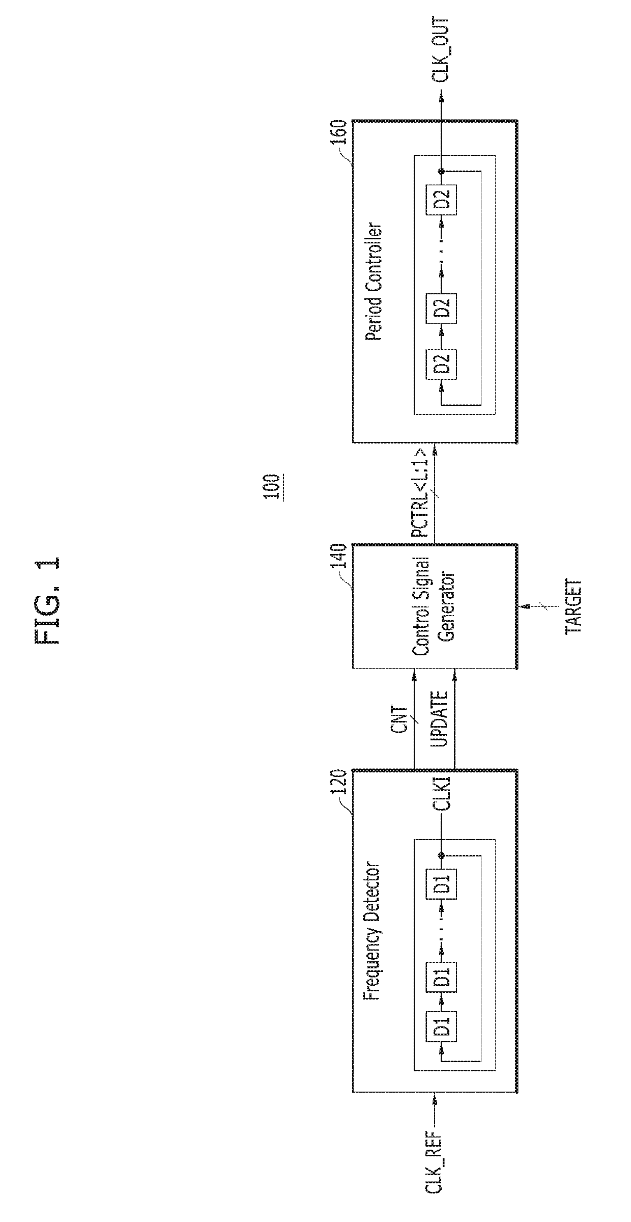
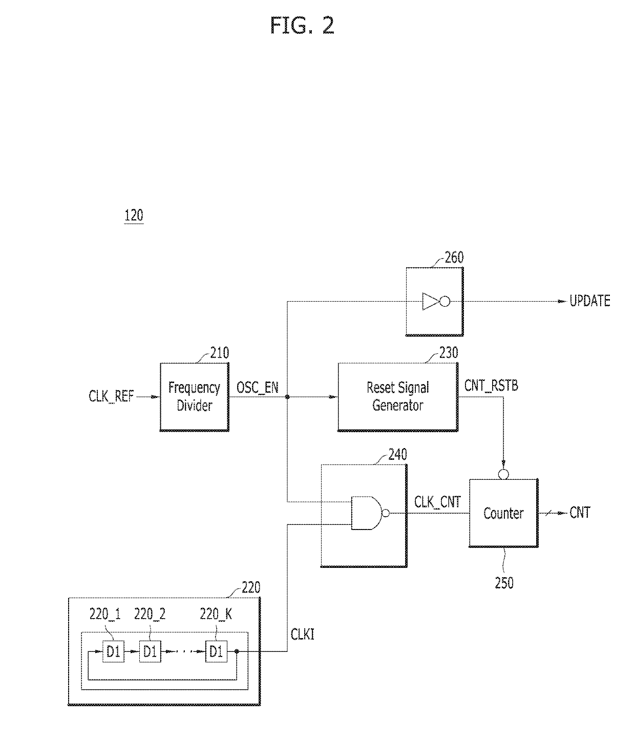
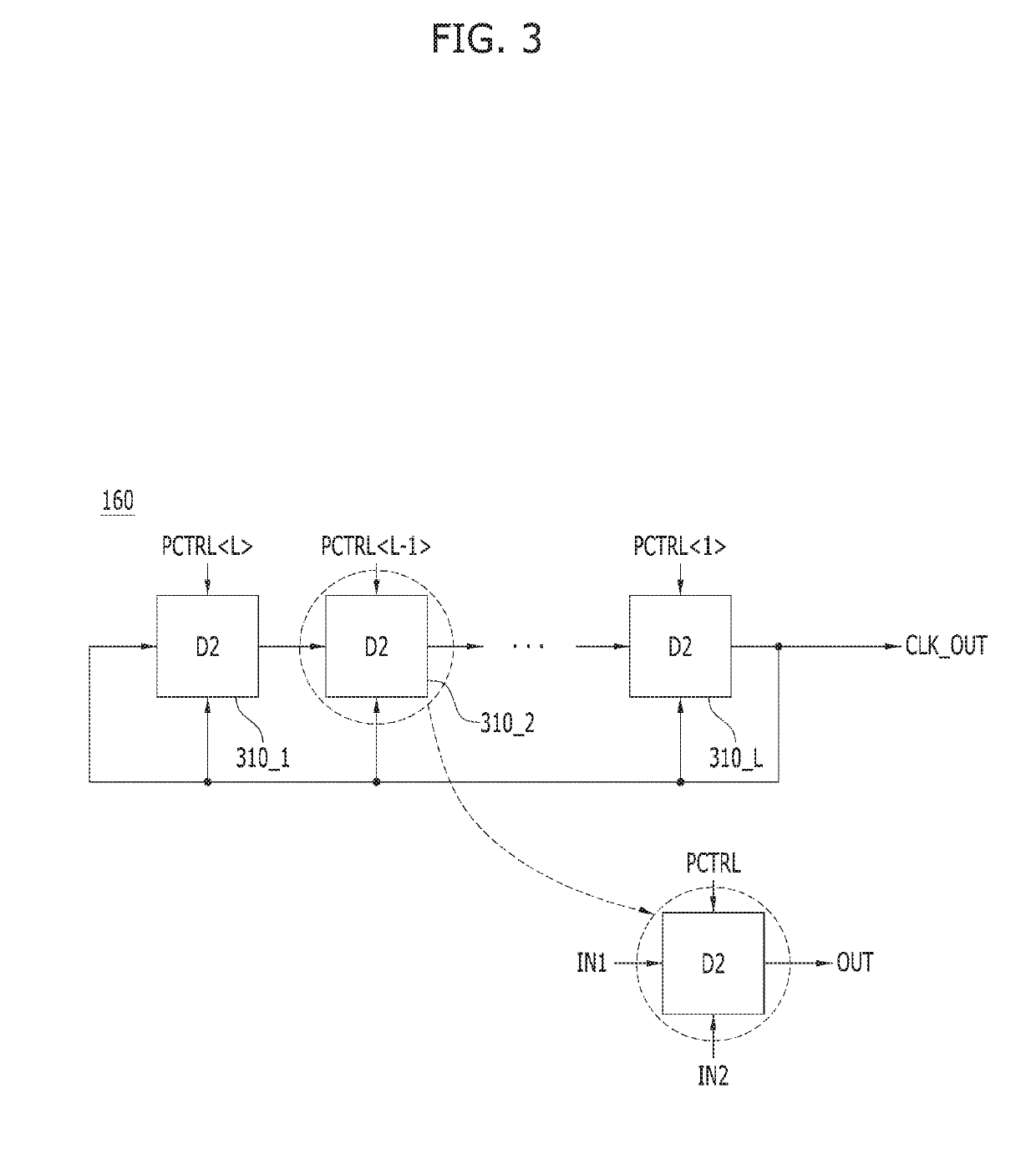
[0021]FIG. 1 is a block diagram illustrating a clock generation circuit 100 in accordance with an embodiment of the present invention.

[0022]Referring to FIG. 1, the clock generation circuit...


PUM


Abstract

A clock generation circuit includes: a frequency detector suitable for generating an internal clock, and generating a counting signal indicating a toggling number of the internal clock during an activation period of an input clock; a control signal generator suitable for generating a plurality of period control signals based on a target signal and the counting signal, the target signal indicating a target frequency of an output clock; and a period controller suitable for generating the output clock based on the period control signals.

Description

CROSS-REFERENCE TO RELATED APPLICATION[0001]The present application claims priority of Korean Patent Application No. 10-2018-0022738, filed on Feb. 26, 2018, which is incorporated herein by reference in its entirety.BACKGROUND1. Field[0002]Various embodiments of the present invention relate to semiconductor technology, and more particularly, to a clock generation circuit of a semiconductor device.2. Description of the Related Art[0003]As the operation speed of semiconductor devices continues to increase, the operation speed of a tester used for testing the semiconductor devices may not keep pace with that increase. For example, whereas the semiconductor devices may operate at frequencies up to approximately 400 megahertz (MHz), the tester may not generate signals exceeding approximately 200 MHz. When the tester operates at approximately 200 MHz in performing the testing, not only does it take a long time to perform the test, but it is not possible to perform a test appropriate for a...

Claims


Application Information

Patent Timeline
IPC IPC(8): H03K5/135H03K21/38H03K23/00G01R31/317
CPCH03K5/135H03K21/38H03K2005/0015G01R31/31727H03K2005/00078H03K23/002G01R31/26G01R23/02H03L7/0814H03L7/087G06F1/04G06F1/10
Inventor PARK, MYEONG-JAEKIM, JI-HWAN
Owner SK HYNIX INC
Why Eureka
Try Eureka