Semiconductor integrated circuit and method for driving the same

a technology of integrated circuits and semiconductors, applied in the direction of digital storage, pulse automatic control, instruments, etc., can solve the problem that the tracking speed may not be optimized during the update process

Active Publication Date: 2013-04-25
SK HYNIX INC
View PDF5 Cites 43 Cited by
  • Summary
  • Abstract
  • Description
  • Claims
  • Application Information

AI Technical Summary

Benefits of technology

[0024]In accordance with an embodiment of the present invention, a semiconductor integrated circuit includes: a delay locked loop (DLL) configured to generate a DLL clock signal by delaying a source clock signal by a first delay time for obtaining a lock, wherein an update period of the DLL is controlled in response to an update period control signal after locking is completed; and an update period controller configured to generate the update period control signal based on a second delay time occurring in a loop path of the DLL in response to the source clock signal and a plurality of control signals provided from the DLL.
[0025]In accordance with another embodiment of the present invention, there is provided a method for driving a semiconductor integrated circuit which includes a DLL configured to generate a DLL clock signal by delaying a source clock by a first delay time for obtaining a lock and an update period controller configured to control an update period of the DLL. The method includes: generating, by the DLL, the DLL clock signal by delaying a source clock signal by the first delay time, wherein the first delay time is variably controlled; controlling, by the update period controller, the update period based on a second delay time that occurs in a loop path of the DLL in a state in which the generating of the DLL clock signal is completed; and performing, by the DLL, an update in response to the controlled update period.

Problems solved by technology

Accordingly, tracking speed may not be optimized during the update process.

Method used


Image

  • Semiconductor integrated circuit and method for driving the same
  • Semiconductor integrated circuit and method for driving the same
  • Semiconductor integrated circuit and method for driving the same

Examples


Embodiment Construction

[0034]Exemplary embodiments of the present invention will be described below in more detail with reference to the accompanying drawings. The present invention may, however, be embodied in different forms and should not be construed as limited to the embodiments set forth herein. Rather, these embodiments are provided so that this disclosure will be thorough and complete, and will fully convey the scope of the present invention to those skilled in the art. Throughout the disclosure, like reference numerals refer to like parts throughout the various figures and embodiments of the present invention.

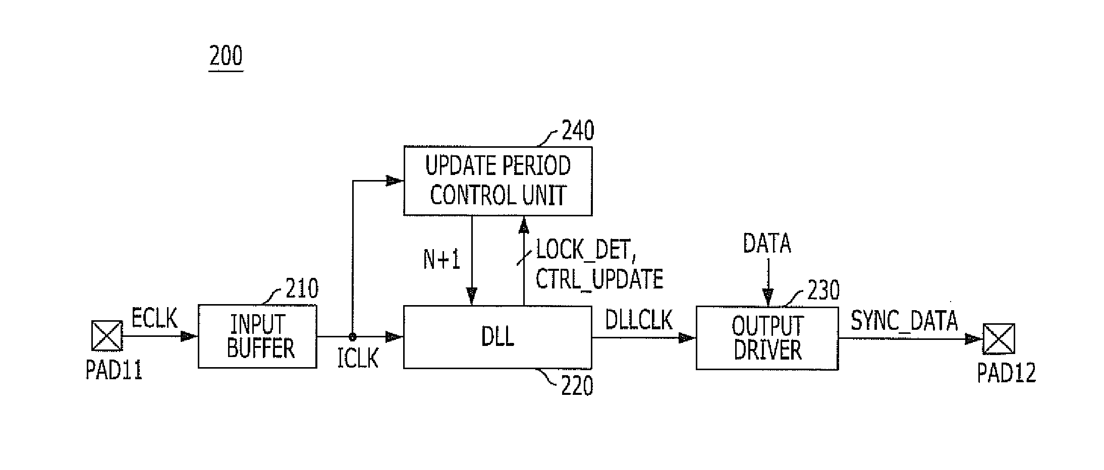
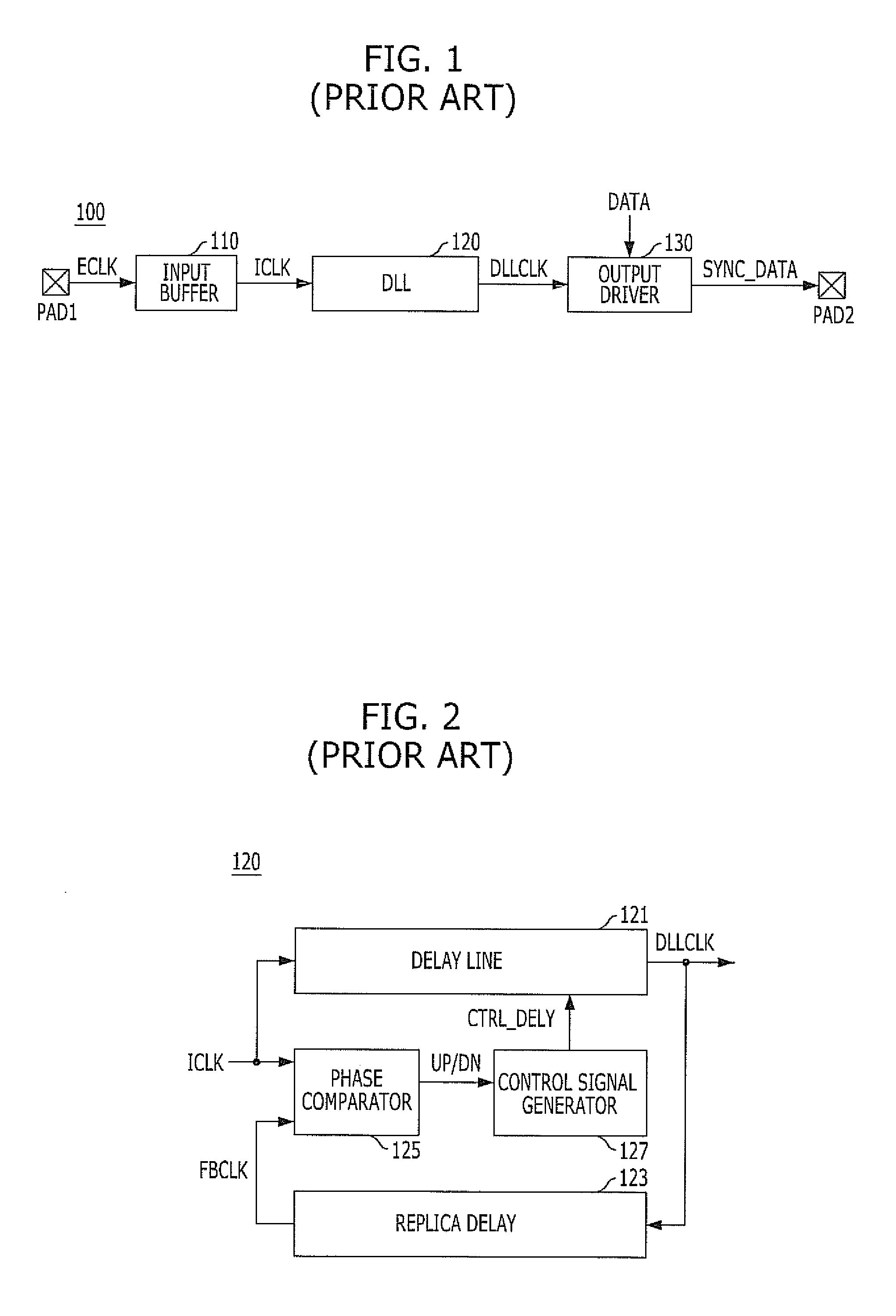
[0035]In the embodiments of the present invention, like names are used for the same signals as those of the conventional semiconductor integrated circuit illustrated in FIGS. 1 to 3, for convenience of explanation.

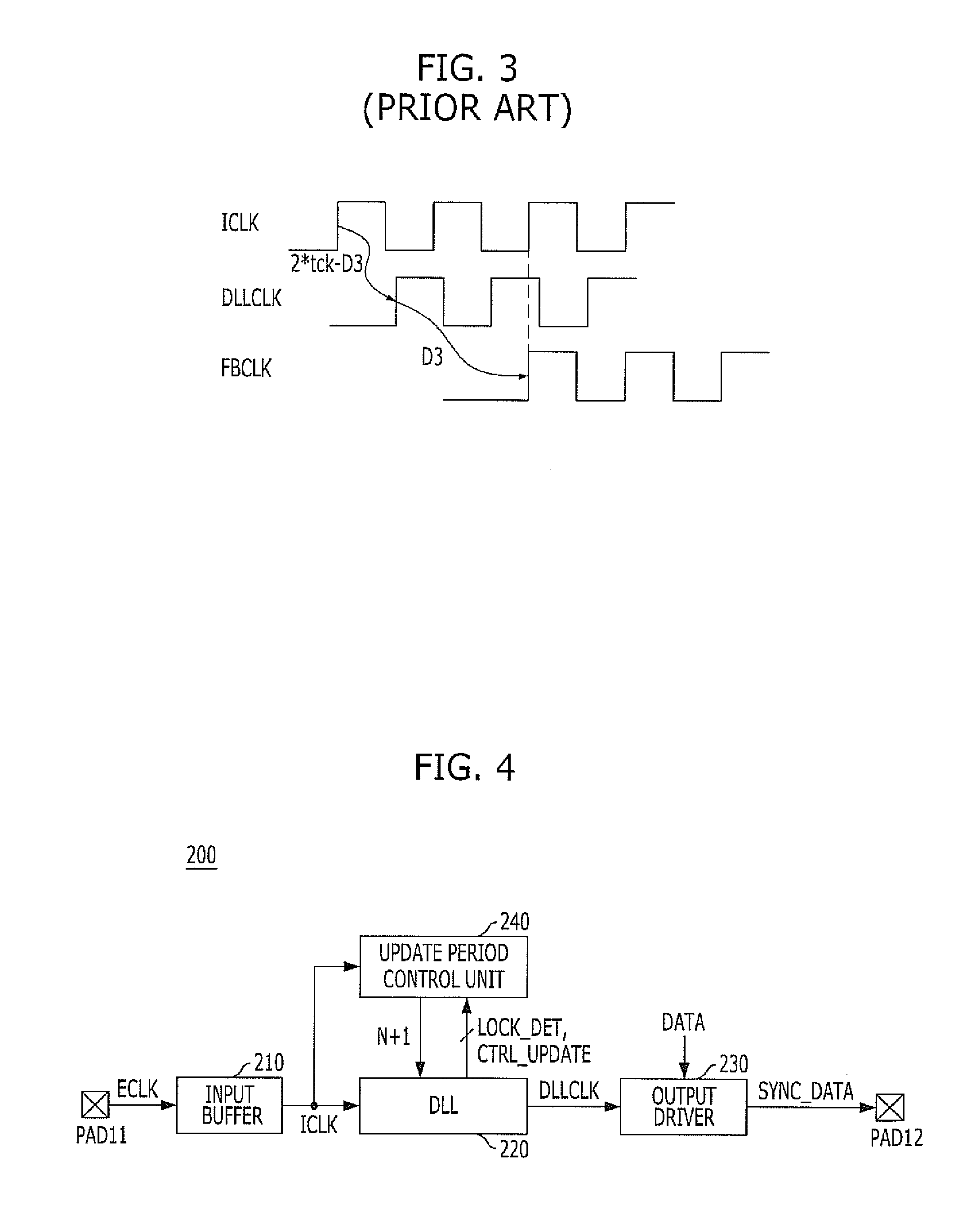
[0036]FIG. 4 is a block configuration diagram of a semiconductor integrated circuit in accordance with an embodiment of the present invention. FIG. 5 is an internal configuration d...


PUM


Abstract

A semiconductor integrated circuit includes: a delay locked loop (DLL) configured to generate a DLL clock signal by delaying a source clock signal by a first delay time for obtaining a lock, wherein an update period of the DLL is controlled in response to an update period control signal after locking is completed; and an update period controller configured to generate the update period control signal based on a second delay time occurring in a loop path of the DLL in response to the source clock signal and a plurality of control signals provided from the DLL.

Description

CROSS-REFERENCE TO RELATED APPLICATIONS[0001]The present application claims priority of Korean Patent Application No. 10-2011-0107587, filed on Oct. 20, 2011, which is incorporated herein by reference in its entirety.BACKGROUND[0002]1. Field[0003]Exemplary embodiments of the present invention relate to semiconductor design technology, and more particularly, to a semiconductor integrated circuit including a delay locked loop (DLL) and a method for driving the same.[0004]2. Description of the Related Art[0005]In general, a semiconductor integrated circuit such as DDR SDRAM (Double Data Rate Synchronous DRAM) includes a DLL configured to equalize the phases of an internal clock signal and an external clock, in order to compensate for time delay caused by an internal circuit when the external clock signal inputted from outside is used inside. More specifically, the DLL receives an external clock signal, compensates for delay components in an actual clock path and data path, and applies ...

Claims


Application Information

Patent Timeline
Patent Type & Authority Applications(United States)
IPC IPC(8): H03L7/095
CPCG11C7/222G11C11/40H03L7/0814G11C2029/0409G11C29/023H03L7/0816G11C8/00
Inventor KIM, YONG-JUKWON, DAE-HANCHOI, HAE-RANGJANG, JAE-MIN
Owner SK HYNIX INC
Why Eureka
Try Eureka