

Internal voltage generating circuit
- Summary
- Abstract
- Description
- Claims
- Application Information
AI Technical Summary
Problems solved by technology
Method used
Image

Examples
Embodiment Construction
[0045] Hereinafter, a semiconductor memory device in accordance with the present invention will be described in detail referring to the accompanying drawings.
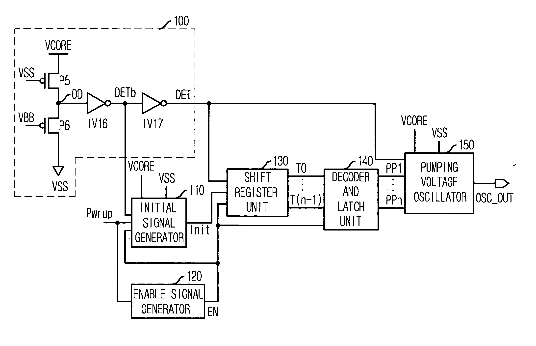
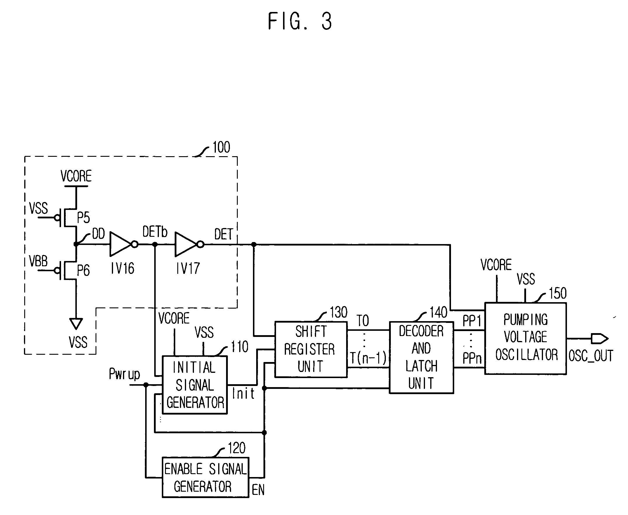
[0046]FIG. 3 is a block diagram of an internal voltage generating circuit in accordance with the present invention.
[0047] The internal voltage generating circuit includes a back bias voltage detector 100, an initial signal generator 110, an enable signal generator 120, a shift register unit 130, a decoder and latch unit 140 and a pumping voltage oscillator 150.
[0048] The back bias voltage detector 100 includes PMOS transistors P5 and P6 and inverters IV16 and IV17. The first and second PMOS transistors P5 and P6, connected in series between a core voltage VCORE node and a ground voltage VSS node, receive the ground voltage VSS or the back bias voltage VBB from each gate. The first inverter IV16 inverts a signal on a node DD and outputs an inverse detecting signal DETb. The second inverter IV17 inverts the inverse detecting s...
PUM
 Abstract
Description
Claims
Application Information