Semiconductor memory element, other elements, and their production methods

Active Publication Date: 2019-09-05
WACOM R&D +1
View PDF0 Cites 0 Cited by
  • Summary
  • Abstract
  • Description
  • Claims
  • Application Information

AI Technical Summary

Benefits of technology

[0038]In the present invention, a protruding structure made of a material having a high etching rate is covered with a partition wall of a material having a relatively low etching rate, is anisotropically cut from the upper side to expose the head portion of the protruding structure, and is selectively removed by etching. Then a high aspect groove is left in the partition wall. By selectively etching the protruding structure, the bottom surface of the exposed groove can have less damage and can accept the interface level by appropriately adjusting the etching conditions. A functional material is deposited and buried in this groove by a film forming method with good step coverage, and it is used for a semiconductor memory element.
[0039]According to the present invention, it is possible to provide the functional material having the high aspect shape in the partition wall on the substrate, and it is effective as a production process of an electronic device. For example, by using an insulator as the partition wall and embedding an electrical conductor in the deep groove formed according to the present invention, an electric wiring can be produced.
[0040]Or, by using a light-impermeable material as the partition wall and embedding a light transmitting material in the deep groove formed according to the present invention, an optical wiring can be p

Problems solved by technology

Also, the ferroelectric substance is a material that is hard to be etched, and then it is difficult to search a masking material, which has high etching selectivity and does not disappear till end of etching.
But, in reality, it is difficult for the slope t

Method used


Image

  • Semiconductor memory element, other elements, and their production methods
  • Semiconductor memory element, other elements, and their production methods
  • Semiconductor memory element, other elements, and their production methods

Examples


Example

[0090]1 substrate (semiconductor substrate)

[0091]2 memory substance

[0092]3 conductor

[0093]4 partition wall

[0094]10 upper surface

[0095]11 side-surface

[0096]12 lower surface

DESCRIPTION OF EMBODIMENTS

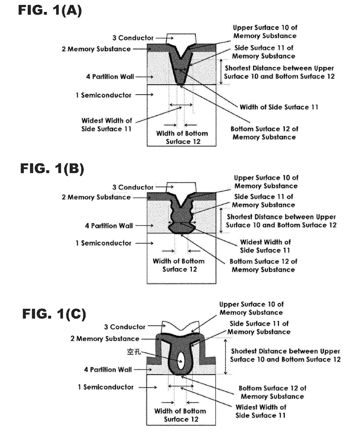
[0097]The memory substance is a solid having a memory function in whole or in part. In other words, the memory substance may be a solid composed of a single material having a memory function, or may be a solid composed of a lamination of a material layer having a memory function and a layer of a material having no memory function. An example of a memory substance is a solid composed of two layers of ferroelectric and paraelectric.

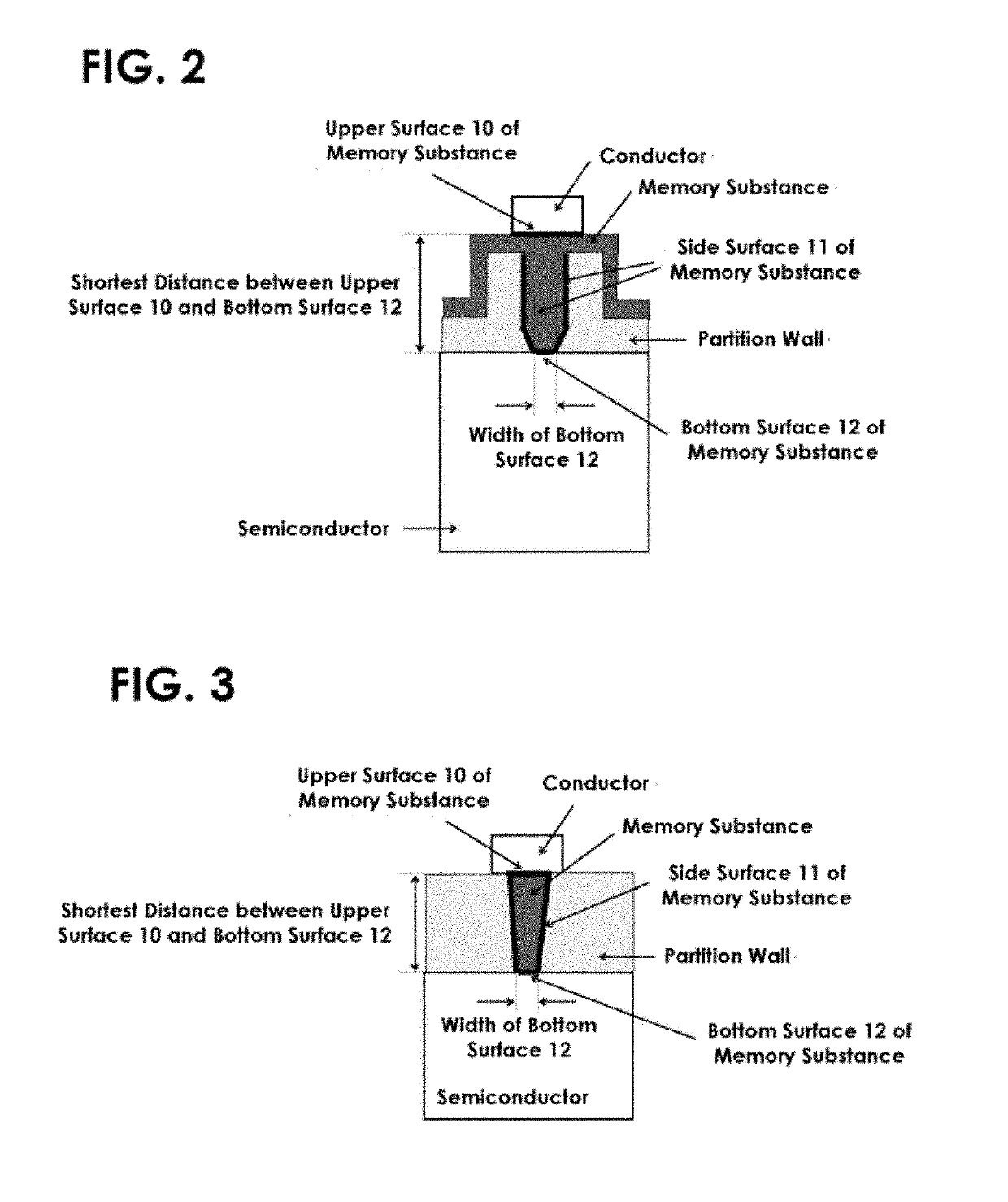
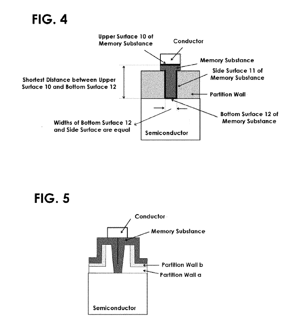
[0098]Embodiments of the present invention are semiconductor memory elements having sectional structures shown in FIGS. 1(a), 1(b) and 1(c). In other words, the semiconductor has a laminated structure, in which a memory substance 2 and a conductor 3 are laminated on a semiconductor substrate 1, and surrounded so that a bottom surface 12 of the memory substance 2 i...


PUM


Abstract

A semiconductor memory element is provided including a laminated structure, in which a memory member and a conductor are superposed on a semiconductor substrate. The memory member has a bottom surface in contact with the semiconductor substrate, an upper surface in contact with the conductor, and side surfaces, which are in contact with and surrounded by a partition wall; the bottom surface of the memory member has a width of equal to or not more than 100 nm; a shortest distance between the conductor and the semiconductor substrate is twice or more of the width of the bottom surface of the memory member; the side surface of the memory member has a width, which is either the same as the width of the bottom surface and constant at any position above the bottom surface, or the widest at a position other than the bottom surface and above the bottom surface.

Description

TECHNICAL FIELD[0001]The present invention relates to a semiconductor memory element and other elements, and their production method. In more detail, the present invention relates to a fine and highly integrated semiconductor memory element and other elements using a structure-like memory substance etc. in the form with a width equal to or smaller than 100 nm, and high aspect ratio, which is a ratio of height to width, equal to or higher than double. The present invention also relates to their production method.BACKGROUND ART[0002]The semiconductor memory element using a functional material finally exhibits its peculiar function, when film thickness of the functional material is larger than several ten nanometers. For example, in the case of a ferroelectric gate transistor using a ferroelectric substance, which is one of the functional materials, memory window decreases and memory function of the element decreases, as a film thickness of the ferroelectric substance decreases (Patent...

Claims


Application Information

Patent Timeline
IPC IPC(8): H01L27/1159H01L29/49H01L29/51H01L29/78H01L21/28H01L21/311H01L29/66
CPCH01L29/40111H01L27/1159H01L29/4983H01L29/516H01L29/78391H01L29/6684H01L21/31116H01L29/6653H01L29/66553H01L21/0337H10B51/20H01L21/3065H10B51/10H10B51/30
Inventor TAKAHASHI, MITSUESAKAI, SHIGEKIKUSUHARA, MASAKITODA, MASAYUKIUMEDA, MASARUSASAKI, YOSHIKAZU
Owner WACOM R&D
Why Eureka
Try Eureka