
Semiconductor packaging structure

a technology of semiconductors and packaging, applied in the direction of semiconductor devices, semiconductor/solid-state device details, electrical apparatus, etc., can solve the problems of high voltage and current rate of change, affecting the safety of elements, and threatening elements' safety, so as to reduce the resistance of the parasiti

Active Publication Date: 2019-09-26
DELTA ELECTRONICS INC
View PDF0 Cites 1 Cited by
  • Summary
  • Abstract
  • Description
  • Claims
  • Application Information

AI Technical Summary

Benefits of technology

The present patent provides a semiconductor packaging structure and a semiconductor power device that reduces parasitic inductor and parasitic resistor effects by minimizing the loop of a bridge arm switch and a decoupling capacitor.

Problems solved by technology

Meanwhile, there are non-ideality parasitic parameters in the whole circuit, and the switching motion will lead to additional peak voltage in elements which endure Vbus such that the safety of the elements will be affected.
However, since there is parasitic inductance in circuit, speeding up the switching speed will lead to high voltage and current rate of change such that peak voltage will generate at two terminals of the element and the safety of the elements will be threatened.
In addition, in special applications (i.e., low voltage and high current), except for parasitic inductance, parasitic impedance among wires will also bring loss and affect the efficiency of the whole system.
In view of the foregoing, problems and disadvantages are associated with existing products that require further improvement.
However, those skilled in the art have yet to find a solution.

Method used


Image

  • Semiconductor packaging structure
  • Semiconductor packaging structure
  • Semiconductor packaging structure

Examples


Embodiment Construction

[0040]The detailed description provided below in connection with the appended drawings is intended as a description of the present examples and is not intended to represent the only forms in which the present example may be constructed or utilized. The description sets forth the functions of the example and the sequence of steps for constructing and operating the example. However, the same or equivalent functions and sequences may be accomplished by different examples.

[0041]Unless otherwise defined herein, scientific and technical terminologies employed in the present disclosure shall have the meanings that are commonly understood and used by one of ordinary skill in the art. Unless otherwise required by context, it will be understood that singular terms shall include plural forms of the same and plural terms shall include singular forms of the same.

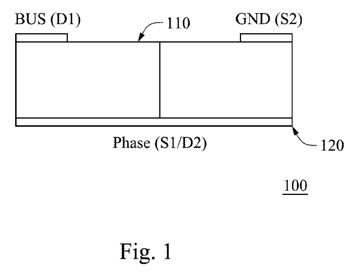
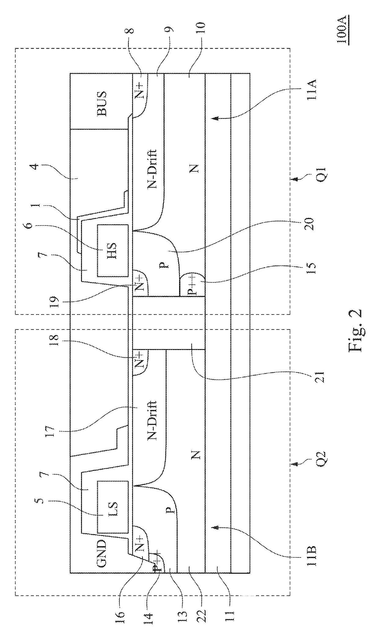
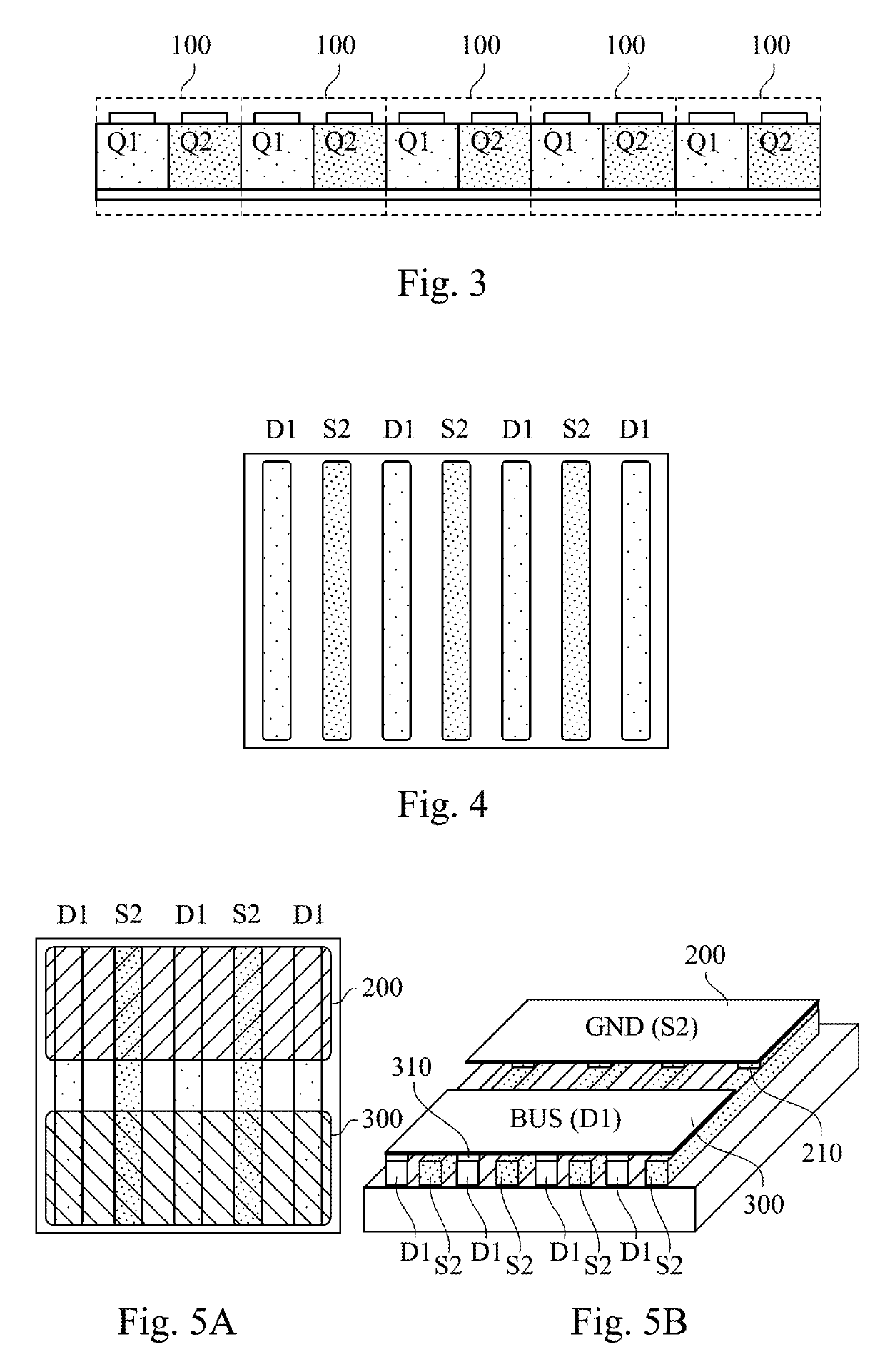
[0042]For minimizing a loop of a bridge arm switch and a decoupling capacitor so as to decrease an effect arose by parasitic inductance...


PUM


Abstract

A semiconductor packaging structure includes a chip, a first pin, a second pin, and a third pin. The chip includes a first surface, a second surface, a first power switch, and a second switch, and both the first power switch and the second switch include a first terminal and a second terminal. The second surface of the chip is opposite to the first surface of the chip. The first pin does not contact to the second pin. The first terminal of the first power switch of the chip is coupled to the first pin, and the second terminal of the first power switch of the chip is coupled to the third pin. The first terminal of the second power switch of the chip is coupled to the third pin, and the second terminal of the second power switch of the chip is coupled to the second pin.

Description

RELATED APPLICATIONS[0001]This application is a Continuation-in-part of U.S. application Ser. No. 15 / 647,278 filed Jul. 12, 2017, which is a Divisional Application of U.S. application Ser. No. 15 / 077,927 filed Mar. 23, 2016, now U.S. Pat. No. 9,755,070, which claims priority to China Application Serial Number 201510154626.2 filed Apr. 2, 2015, which is herein incorporated by reference.BACKGROUNDField of Invention[0002]The present invention relates to a packaging structure. More particularly, the present invention relates to a semiconductor packaging structure.Description of Related Art[0003]Power supplies are a core member of energy conversion and also an indispensable device in the current electric power industry, electronics industry, electric machinery industry and energy industry. Important characteristics of supplies are energy conversion efficiency, power intensity, heat dissipation, and so on. The qualities of the foregoing characteristics will affect the performance of a sys...

Claims


Application Information

Patent Timeline
IPC IPC(8): H01L29/78H01L23/50H01L23/00
CPCH01L29/402H01L2924/19104H01L29/1083H01L29/41766H01L24/20H01L29/7816H01L29/7826H01L2224/18H01L23/50H01L2224/04105H01L24/24H01L29/1095H01L27/088H01L23/642H01L2924/19106H01L2924/181H01L24/40H01L2224/40095H01L2924/00012
Inventor CAI, CHAO-FENGZENG, JIAN-HONGLI, ZENGXIN, XIAO-NI
Owner DELTA ELECTRONICS INC
Learn More