

Voltage regulator
- Summary
- Abstract
- Description
- Claims
- Application Information
AI Technical Summary
Benefits of technology
Problems solved by technology
Method used
Image

Examples
Embodiment Construction
[0020]Embodiments of the present invention will hereinafter be described with reference to the accompanying drawings.
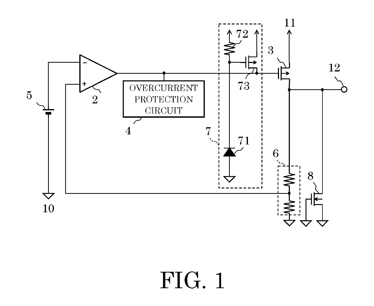
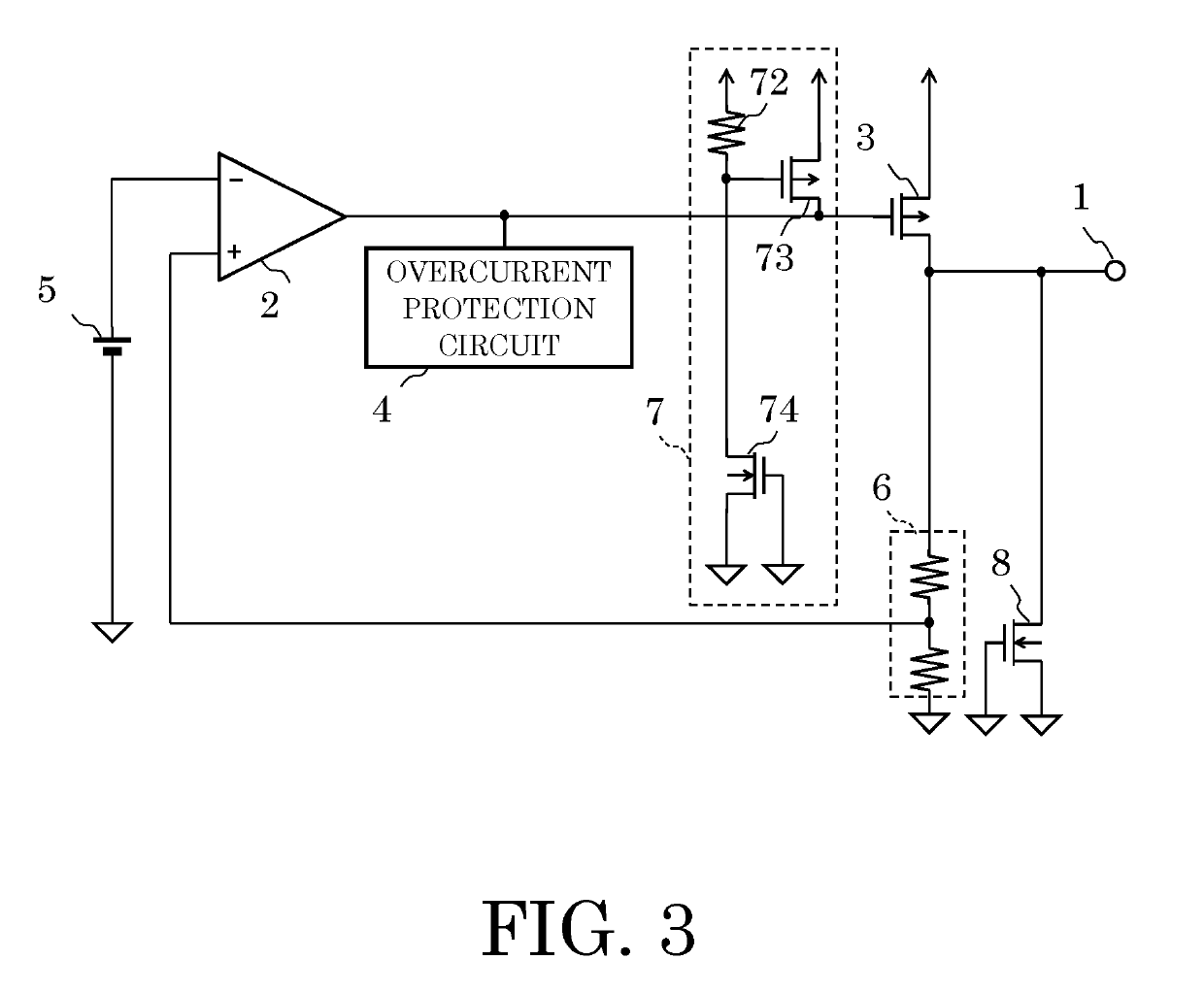
[0021]FIG. 1 is a circuit diagram illustrating a voltage regulator according to an embodiment of the present invention.
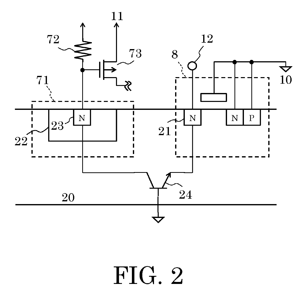
[0022]The voltage regulator according to the embodiment has an error amplifier circuit 2, a PMOS transistor 3 being an output transistor, an overcurrent protection circuit 4, a reference voltage circuit 5, a resistance circuit 6, a protection circuit 7, an NMOS transistor 8 being a clamp circuit, and an output terminal 12. The protection circuit 7 has a diode 71, a resistor 72, and a PMOS transistor 73. The NMOS transistor 8 is an ESD protection element. Although described later, the protection circuit 7 is constructed to include a drain region of the NMOS transistor 8.
[0023]A description will next be made of connections of the voltage regulator according to the embodiment.
[0024]The error amplifier circuit 2 has an inversion input terminal connected t...
PUM
 Abstract
Description
Claims
Application Information