Sibn film for conformal hermetic dielectric encapsulation without direct RF exposure to underlying structure material

a dielectric encapsulation and conformal hermetic technology, applied in the direction of coating, chemical vapor deposition coating, metallic material coating process, etc., can solve the problem that memory materials are also sensitive to plasma damag

Active Publication Date: 2019-10-24
APPLIED MATERIALS INC
View PDF5 Cites 8 Cited by
  • Summary
  • Abstract
  • Description
  • Claims
  • Application Information

AI Technical Summary

Problems solved by technology

Additionally, memory materials are also sensitive to plasma damage.

Method used


Image

  • Sibn film for conformal hermetic dielectric encapsulation without direct RF exposure to underlying structure material
  • Sibn film for conformal hermetic dielectric encapsulation without direct RF exposure to underlying structure material

Examples


Embodiment Construction

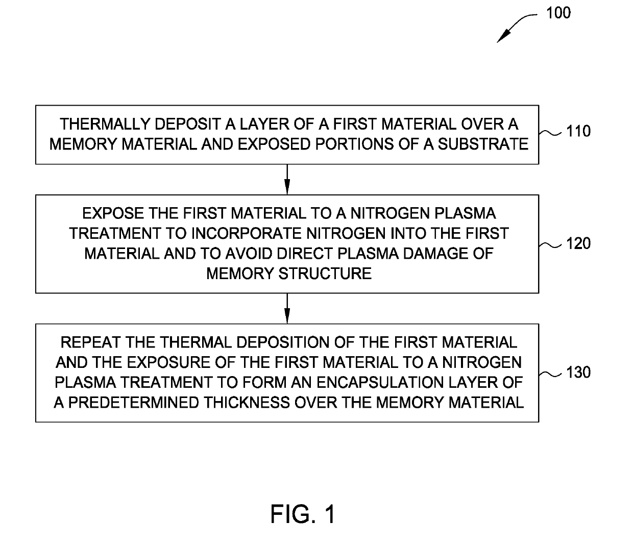
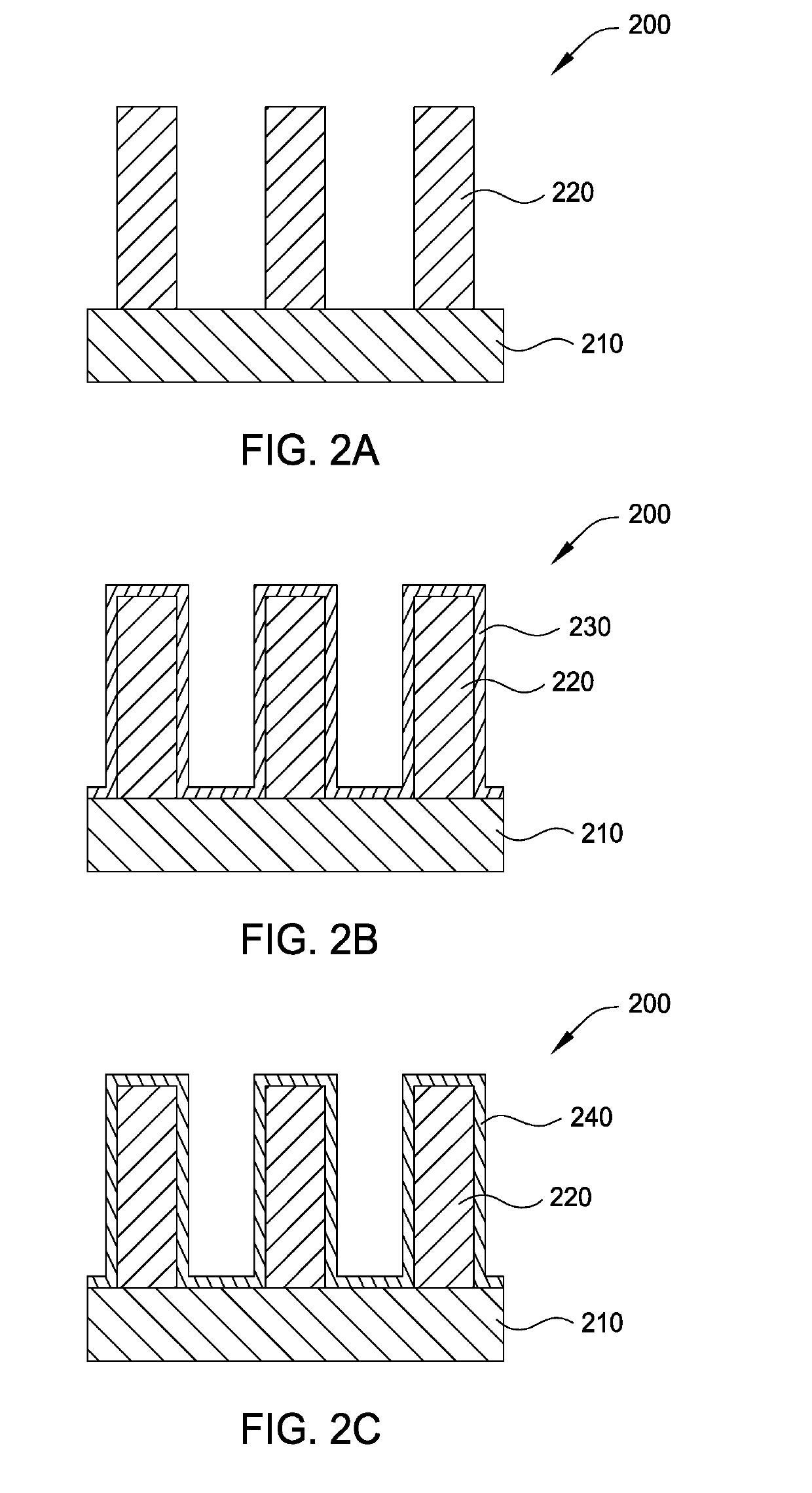
[0012]Embodiments disclosed herein relate to methods for forming memory devices, and more specifically to improved methods for forming a dielectric encapsulation layer over a memory material in a memory device. In one embodiment, the method includes thermally depositing a first material over a memory material at a temperature less than the temperature of the thermal budget of the memory material, exposing the first material to nitrogen plasma to incorporate nitrogen in the first material, and repeating the thermal deposition and nitrogen plasma operations to form a hermetic, conformal dielectric encapsulation layer over the memory material. Thus, a memory device having a hermetic, conformal dielectric encapsulation layer over the memory material is formed.

[0013]FIG. 1 is a process flow 100 for depositing a dielectric encapsulation layer. The process flow 100 begins at operation 110 by thermally depositing a layer of a first material over a memory material and exposed portions of a s...


PUM

PropertyMeasurementUnit
temperatureaaaaaaaaaa
thicknessaaaaaaaaaa
thicknessaaaaaaaaaa

Abstract

Embodiments disclosed herein relate to methods for forming memory devices, and more specifically to improved methods for forming a dielectric encapsulation layer over a memory material in a memory device. In one embodiment, the method includes thermally depositing a first material over a memory material at a temperature less than the temperature of the thermal budget of the memory material, exposing the first material to nitrogen plasma to incorporate nitrogen in the first material, and repeating the thermal deposition and nitrogen plasma operations to form a hermetic, conformal dielectric encapsulation layer over the memory material. Thus, a memory device having a hermetic, conformal dielectric encapsulation layer over the memory material is formed.

Description

BACKGROUNDField[0001]Embodiments disclosed herein relate to methods for forming memory devices, and more specifically to methods for forming a dielectric encapsulation layer over a high aspect ratio material, such as a transition metal based material of a memory cell device.Description of the Related Art[0002]Nonvolatile Random Access Memory (RAM) devices generally include millions of memory cells containing transition metal based materials such as copper (Cu), useful for memory storage in 0(s) and 1(s). Dielectrically separating memory material from metal interconnects that manage the memory state contributes to maximizing operation of the memory cells. Deposition of dielectric encapsulation materials is typically achieved by high-temperature, plasma treatment processes, such as Plasma Enhanced-CVD (PECVD). However, the memory materials have a fixed thermal budget to avoid thermal damage. Additionally, memory materials are also sensitive to plasma damage. If the sensitive memory ma...

Claims


Application Information

Patent Timeline
Patent Type & Authority Applications(United States)
IPC IPC(8): H01L21/02C23C16/34H01L21/768
CPCH01L21/0217H01L21/02252H01L21/0228H01L21/02211H01L21/76834C23C16/345H01L21/02274H01L21/76826H01L21/76876H01L21/76801H01L21/324H10B69/00C23C16/38
Inventor GADRE, MILINDMUKHERJEE, SHAUNAKJHA, PRAKET P.PADHI, DEENESHDUAN, ZIQINGMALLICK, ABHIJIT B.
Owner APPLIED MATERIALS INC
Why Eureka
Try Eureka