
Device Having a Reinforcement Layer and Method for Producing a Device

Active Publication Date: 2019-10-31
OSRAM OLED
View PDF0 Cites 0 Cited by
  • Summary
  • Abstract
  • Description
  • Claims
  • Application Information

AI Technical Summary

Benefits of technology

The invention provides a device that is stable against temperature fluctuations and can be produced inexpensively. The device has a carrier plate, a shaped body, and a reinforcement layer. The shaped body encloses an electronic component and is made of a material with a larger coefficient of thermal expansion than the carrier plate and reinforcement layer. This prevents deformation of the shaped body due to temperature fluctuations. The carrier plate and reinforcement layer adjoin the shaped body at least in places and are configured to absorb stresses on both sides. This prevents asymmetrical deformation of the shaped body, such as lateral tilting of a side surface. The carrier plate and reinforcement layer can be produced with similar bending strength to prevent asymmetric deformation of the shaped body. The shaped body shows a smaller product of its layer thickness and modulus of elasticity than the carrier plate and reinforcement layer to ensure mechanical stability.

Problems solved by technology

In the case of a device which has a component embedded in a casting body and, in particular, arranged on a printed circuit board, temperature fluctuations often lead to deformations due to different expansion coefficients of the shaped body and the printed circuit board.
In order to reduce the deformation, materials of the casting body and the printed circuit board can be adapted to each other, but this leads to a strong restriction in the choice of materials.

Method used


Image

  • Device Having a Reinforcement Layer and Method for Producing a Device
  • Device Having a Reinforcement Layer and Method for Producing a Device
  • Device Having a Reinforcement Layer and Method for Producing a Device

Examples


Embodiment Construction

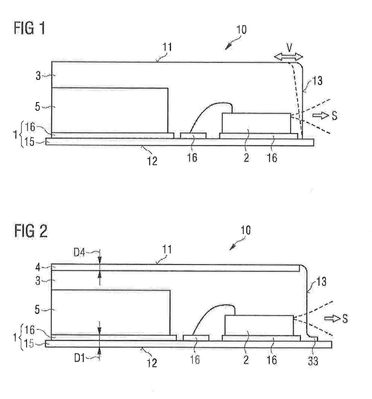
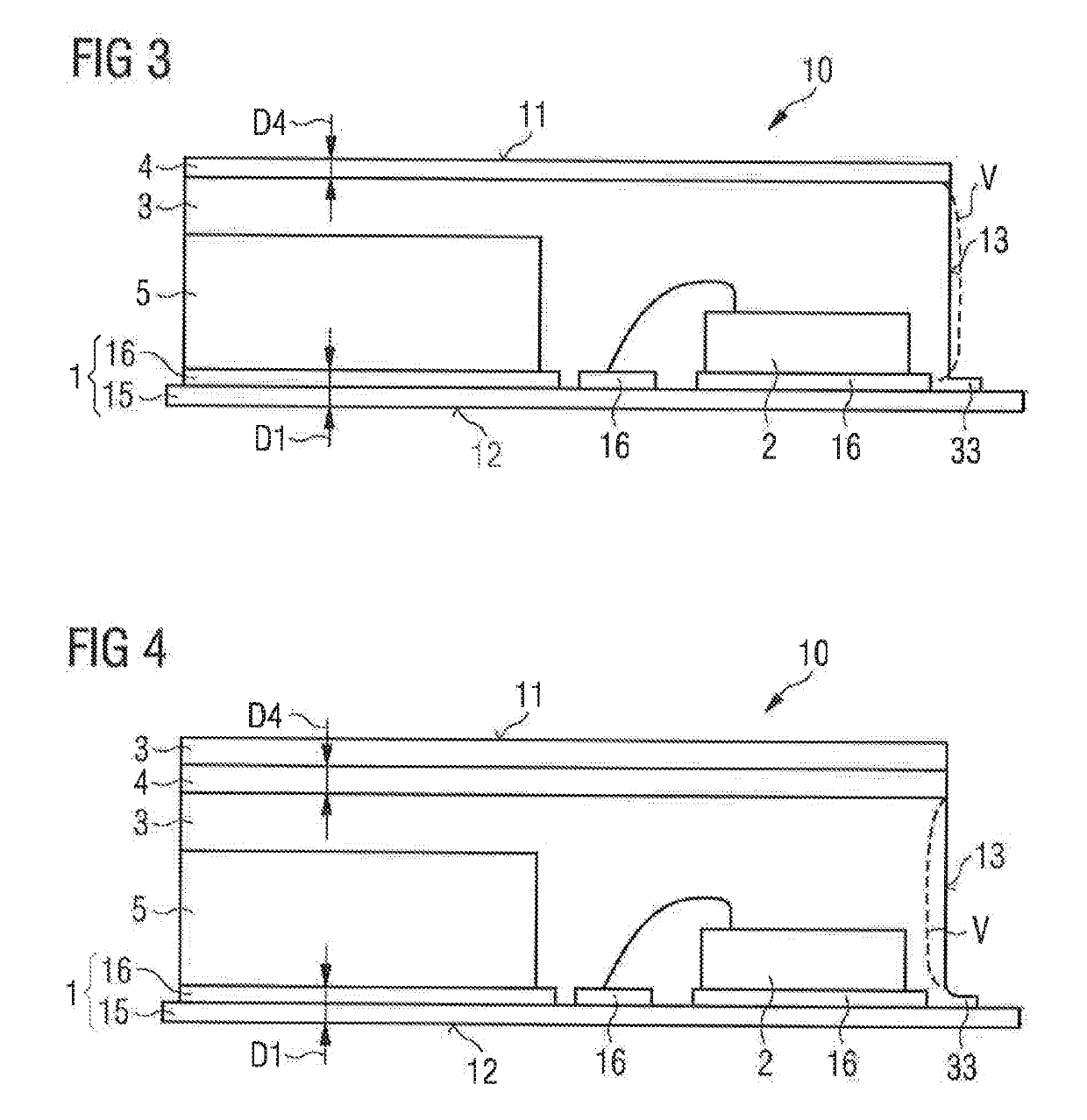
[0032]FIG. 1 schematically shows a comparison exemplary embodiment of a device 10 having a carrier plate 1, an electronic component 2 and a shaped body 3.

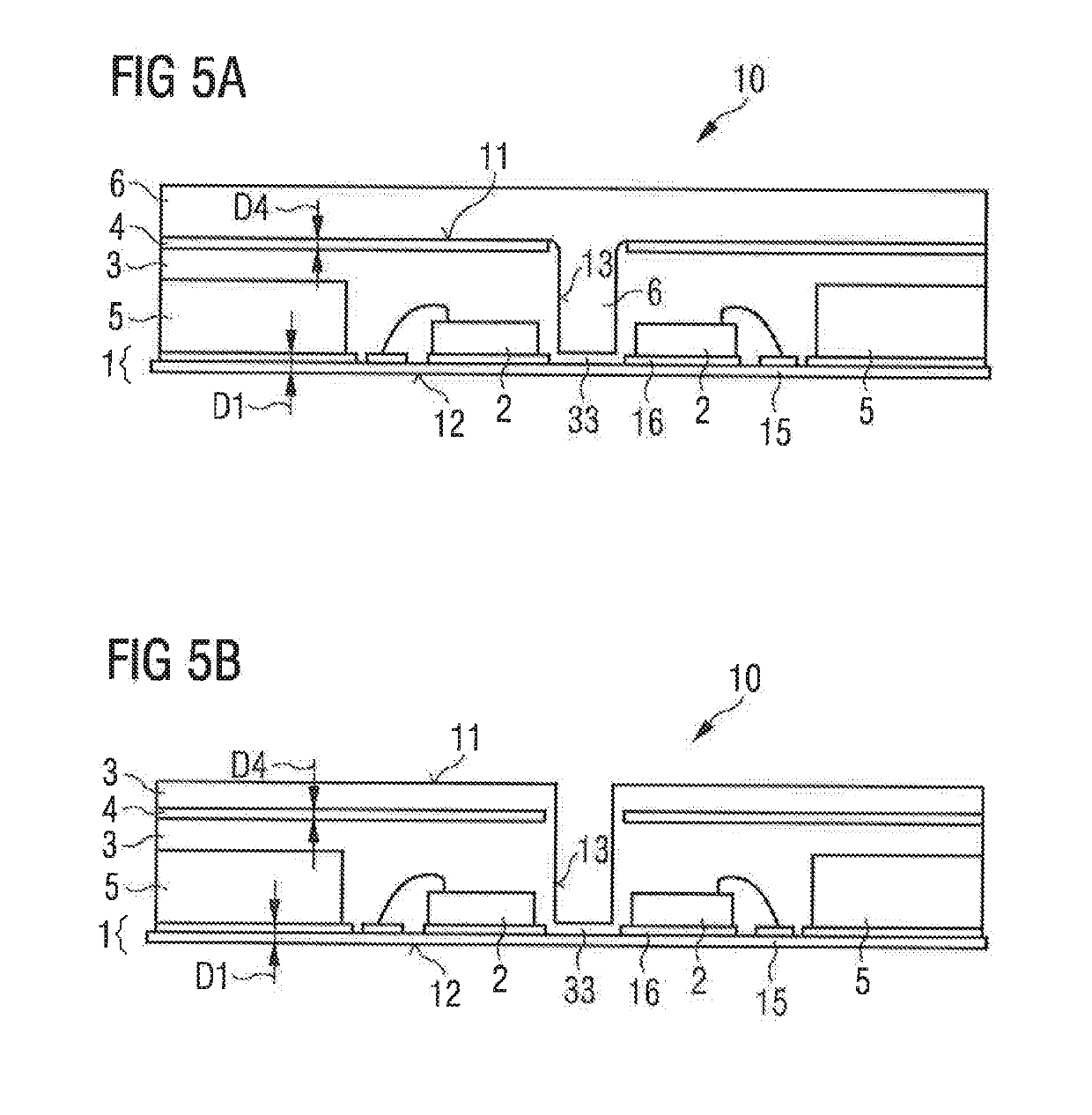
[0033]The carrier plate 1 has a base body 15 and electrical conductor tracks 16 arranged thereon. The carrier plate 1 is for instance a printed circuit board. The electronic component 2 is arranged on the carrier plate 1 and electrically connected to the electrical conductor tracks 16. FIG. 1 shows that the component 2 is electrically connectable partly via a front side facing away from carrier plate 1 and partly via a rear side of the component 2 facing away from carrier plate 1. In particular, an electrical connection point on the front side of the component 2 is electrically connected to one of the conductor tracks 16 via a wire connection. The rear side is formed in particular as a mounting surface of the component 2 and can have one or more electrical connection points which can be electrically connected to one or more electri...


PUM


Abstract

A device having a reinforcement layer and a method for producing a device are disclosed. In an embodiment a device includes a carrier plate, an electronic component, a shaped body and a reinforcement layer, wherein the electronic component is laterally enclosed by the shaped body, wherein, in a vertical direction, the electronic component is arranged between the carrier plate and the reinforcement layer, wherein the shaped body has a thermal expansion coefficient which is at least three times as large as a thermal expansion coefficient of the carrier plate and at least three times as large as a thermal expansion coefficient of the reinforcement layer, and wherein the carrier plate and the reinforcement layer adjoin the shaped body at least in places and are configured to reduce deformation of the shaped body in an event of temperature fluctuations.

Description

[0001]This patent application is a national phase filing under section 371 of PCT / EP2018 / 056064, filed Mar. 12, 2018, which claims the priority of German patent application 102017105235.6, filed Mar. 13, 2017, each of which is incorporated herein by reference in its entirety.TECHNICAL FIELD[0002]A device having a reinforcement layer and its production are specified.BACKGROUND[0003]In the case of a device which has a component embedded in a casting body and, in particular, arranged on a printed circuit board, temperature fluctuations often lead to deformations due to different expansion coefficients of the shaped body and the printed circuit board. In particular, the casting body is deformed more strongly than the embedded component or the printed circuit board. In order to reduce the deformation, materials of the casting body and the printed circuit board can be adapted to each other, but this leads to a strong restriction in the choice of materials.SUMMARY OF THE INVENTION[0004]Emb...

Claims


Application Information

Patent Timeline
IPC IPC(8): H01S5/022H05K1/18H01S5/06
CPCH01S5/0612H05K2201/10106H01S5/02228H05K1/181H05K2201/10121H01S5/02208H01L33/54H01L33/56H01S5/02234
Inventor PINDL, MARKUSSTICH, BERNHARDWOJCIK, ANDREAS
Owner OSRAM OLED
Learn More