
Analog to digital converter having a non-linear ramp voltage

Inactive Publication Date: 2009-11-03
STMICROELECTRONICS RES & DEV
View PDF5 Cites 16 Cited by
  • Summary
  • Abstract
  • Description
  • Claims
  • Application Information

AI Technical Summary

Benefits of technology

[0025]Such a DAC generates a non-linear ramp voltage without many additional components being required. This may reduce the complexity of manufacture as compared to prior art arrangements. It may also reduce the power consumption of the DAC compared to prior art arrangements for the production of non-linear ramps.
[0027]The incremental step may be varied between clock signals. The incremental step may be zero at a low digital ramp code, and typically for the first one hundred or less digital ramp codes generated, and preferably for the first fifty or less digital ramp codes generated. This overcomes the problem associated with ADC quantization noise dominating at low pixel illuminations.
[0028]Either or both of the first and second counters may comprise shift registers. Shift registers have the advantage that they do not take up a large area since, for example, no LUTs are required which means that it is inexpensive to produce. In addition, they have low power consumption. Furthermore, no gain adjustment is needed. This makes it simple to implement.

Problems solved by technology

This involves dopant implantations that result in the substrate being unsuitable for high performance transistor manufacture.
Additionally, pixel photon shot noise is the dominant noise mechanism in CMOS image sensors when a pixel is subject to strong illumination as the number of photons detected varies due to the quantized nature of photons.
As the level of illumination incident upon a pixel increases, this relationship changes and photon shot noise dominates the total system noise.
This either limits the amount of device area available for sensing applications, or will increase the size of the die with an attendant increase in the cost of the sensor.
The fabrication of ROM on the device will increase the complexity of manufacture of the device, with the inherent increased risk of device failure.
Additionally, a typical ALU requires a significant amount of current to operate at high speeds.
This approach a number of disadvantages associated with it, for example, discontinuities exist at poles associated with the junctions between linear regions.
These discontinuities introduce artifacts or distortions in images where the pixel output voltage corresponds closely to the coding value at which the discontinuity occurs.

Method used


Image

  • Analog to digital converter having a non-linear ramp voltage
  • Analog to digital converter having a non-linear ramp voltage
  • Analog to digital converter having a non-linear ramp voltage

Examples


Embodiment Construction

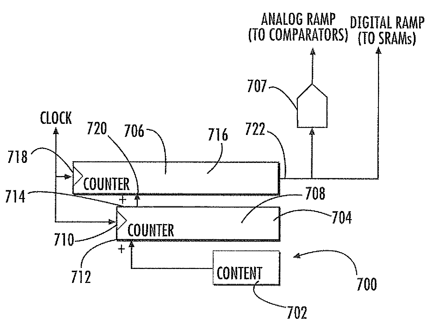
[0044]Referring now to FIG. 7, a non-linear, typically quadratic digital ramp generator 700 comprises a memory device 702, an incremental counter 704, a ramp counter 706, and a DAC 707. In a preferred embodiment, the counters 704, 706 are shift registers. The incremental counter 704 comprises a processor 708, a clock input 710, an additive input 712 and an output 714.

[0045]The ramp counter 706 comprises a processor 716, a clock input 718, an incremental input 720 and an output 722. The incremental counter 704 and the ramp counter 706 receive a clock signal from the same clock (not shown) at their respective clock inputs 710, 718. Receipt of the clock signal triggers the processor 716 of the ramp counter 706 to output a ramp code RAMP, currently stored at the ramp counter 706, to a DAC and a data storage device via the output 722.

[0046]Typically, the ramp counter will have an initial code of zero, although non-zero initial codes are possible. Receipt of the clock signal triggers the ...


PUM


Abstract

An analog to digital converter (ADC) includes a digital ramp generator, an analog voltage comparator, a digital to analog converter (DAC) and a data storage device. The digital ramp generator includes first and second counters. The counter outputs an incremental code to a second counter so that the output code of the second counter varies by the incremental code. The second counter outputs a digital ramp code to respective inputs of the DAC and the data storage device. The DAC outputs an analog voltage to an input of the analog voltage comparator which switches logic states when the output analog voltage of the DAC equals an input voltage received at the analog voltage comparator. The data storage device stores a code of the digital ramp code received at the data storage device at the switching of the logic state of the analog voltage comparator. The first counter varies the incremental code by an incremental step in response to a clock signal.

Description

FIELD OF THE INVENTION[0001]The invention relates to an analog to digital converter (ADC) having a non-linear ramp voltage for use in an image sensor. More particularly, but not exclusively, the invention relates to an ADC having a smooth non-linear ramp voltage for use in a complementary metal oxide semiconductor (CMOS) based image sensor.BACKGROUND OF THE INVENTION[0002]There are two types of commonly used image sensors, Charge Coupled Devices (CCDs) and (CMOS) sensors. Both CCD and CMOS image sensors convert photons into electrons via the interaction of photons with a semiconductor, typically silicon.[0003]CCD sensors transfer charge within the silicon using electric fields and require high charge transfer efficiency (CTE), close to 100%. Consequently, the manufacturing of CCD sensor is tailored to maximize or increase the CTE associated with the device. This involves dopant implantations that result in the substrate being unsuitable for high performance transistor manufacture.[0...

Claims


Application Information

Patent Timeline
IPC IPC(8): H03M1/58
CPCH03M1/464H04N5/335H04N5/217H04N23/81H04N25/00
Inventor DANESH, SEYED
Owner STMICROELECTRONICS RES & DEV
Learn More