Ceramic liner with integrated faraday shielding

a ceramic liner and faraday shielding technology, applied in the field of semiconductor manufacturing, can solve problems such as problematic heating of ceramic liner, achieve the effects of improving the adhesion of sputtered materials, preventing particle spallation, and increasing the life of ceramic liner

Inactive Publication Date: 2019-11-07
ASMPT NEXX INC
View PDF0 Cites 2 Cited by
  • Summary
  • Abstract
  • Description
  • Claims
  • Application Information

AI Technical Summary

Benefits of technology

[0009]Systems and methods herein include a component comprising an integrated liner with a Faraday shield. With such integration, a ceramic liner can be held at a constant temperature to prevent particle spallation. The Faraday shield is used to heat the ceramic liner to prevent particle production in a corresponding etch chamber. Such heating can include pre-heating prior to substrate processing to avoid thermal cycling of the liner in the presence of a substrate.
[0010]The liner with integrated Faraday shield herein can increase liner lifetime before needing to be cleaned because of improved adhesion of sputtered material on the liner. Etch uniformity can be improved by a suitable selection of Faraday shielding pattern.

Problems solved by technology

One constant challenge with fabrication of semiconductors is preventing contamination of devices and substrates.
Such heating of the ceramic liner is problematic because particle spallation occurs due to thermal cycling of the liner.

Method used


Image

  • Ceramic liner with integrated faraday shielding
  • Ceramic liner with integrated faraday shielding
  • Ceramic liner with integrated faraday shielding

Examples


Embodiment Construction

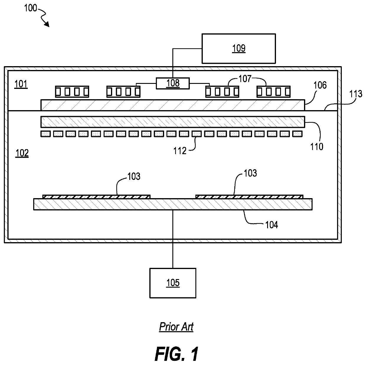
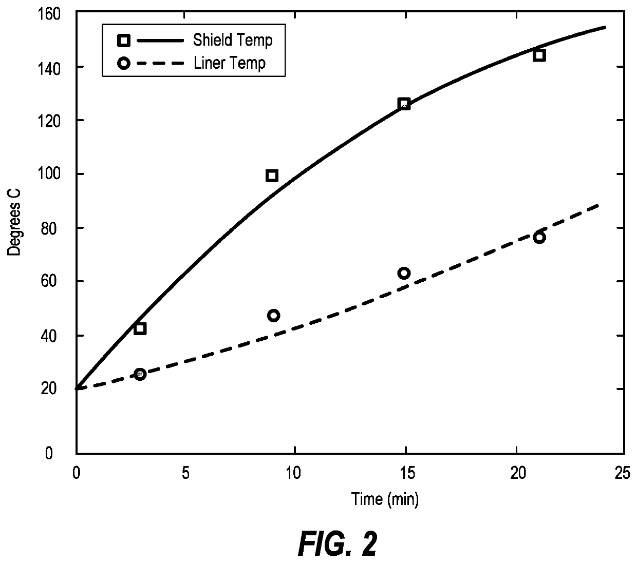
[0021]Now referring to the drawings, FIG. 1 illustrates a conventional plasma processing chamber 100 (also known as an “etch chamber”), which includes chuck support member 104, semiconductor substrates in the form of wafers 103, RF high frequency bias generator 105, a power source including RF low frequency ICP generator 109, matching network 108 and ICP coils 107, a first sub-chamber 101 (which can be at atmospheric pressure / atmosphere, and so is hereafter denoted “atmosphere chamber”), a second sub-chamber 102 (which may be subjected to a vacuum and hence is hereafter denoted “vacuum chamber”), ceramic liner 110 and conventional Faraday shield 112. The plasma processing chamber 100 is divided into the first and second sub-chambers 101, 102 by a partition separating vacuum from atmosphere, the partition including both a metal wall 113 and a ceramic window 106 located in the metal wall 113 and positioned between the power source and the ceramic liner 110. The Faraday shield 112 is l...


PUM


Abstract

A plasma processing system for processing a semiconductor substrate, the system including a plasma processing chamber having a substrate support member configured for receiving a semiconductor substrate within the plasma processing chamber; a process gas delivery system configured to deliver process gas to the plasma processing chamber; a power source configured to energize process gas within the plasma processing chamber to create plasma; and a component positioned between the power source and the substrate support member, the component including a ceramic liner and a Faraday shield in contact with a surface of the ceramic liner.

Description

CROSS REFERENCE TO RELATED APPLICATION[0001]This application claims priority from U.S. Provisional Application Ser. No. 62 / 666,361, filed May 3, 2018, the entire disclosure of which is hereby incorporated by reference.BACKGROUND OF THE INVENTION[0002]This disclosure relates to semiconductor manufacturing. There are many process steps executed to fabricate integrated circuits. Various patterning, deposition, and cleaning steps are executed to fabricate and create packages for integrated circuits. Such steps can include dry cleaning operations in which plasma is used to clean or remove materials from a substrate. One constant challenge with fabrication of semiconductors is preventing contamination of devices and substrates.[0003]Techniques herein provide particle reduction systems and methods. This includes particle reduction in plasma cleaning systems such as an inductively coupled plasma (ICP) sputter clean etch chamber of a physical vapor deposition (PVD) tool. During etch processi...

Claims


Application Information

Patent Timeline
Patent Type & Authority Applications(United States)
IPC IPC(8): H01J37/32H01L21/67
CPCH01L21/67069H01J37/32477H01J37/32807H01J2237/334H01J37/321H01J2237/0266H01J37/32467H01J2237/24585
Inventor GOODMAN, DANIEL
Owner ASMPT NEXX INC
Why Eureka
Try Eureka