Thin film forming method

Pending Publication Date: 2019-11-14
ASM IP HLDG BV
View PDF1 Cites 186 Cited by
  • Summary
  • Abstract
  • Description
  • Claims
  • Application Information

AI Technical Summary

Benefits of technology

The patent text describes a method and apparatus for processing substrates that can reduce the amount of gas wasted during a chemical vapor deposition (CVD) process. Specifically, by using a gas bypass path that also removes excess gas from the reaction chamber, the amount of unreacted gas can be minimized. This results in a more efficient use of the source gas and reactive gas, reducing costs and improving the quality of the substrate processing.

Problems solved by technology

Semiconductor substrate processing processes, such as a deposition or etching process, have become more complicated as semiconductor technology has advanced, and thus various types of chemicals are increasingly being used as raw materials.
When heterologous chemicals with high reactivity are used, equipment operation may be disrupted by reaction byproducts.
For example, reaction byproducts may remain in an exhaust line as solids, and these residual solids may reduce exhaust efficiency and cause malfunctions of internal components such as valves, pressure gauges, and the like.
In addition, solids remain in a scrubber or exhaust pump, which collects harmful chemicals before being exhausted to the air, and thus, when overall operation of a substrate processing apparatus is stopped, it may cause big problems in apparatus operation and productivity improvement.
When this method is used, however, a much greater amount of source gas than needed in reaction may be wasted, and a much larger amount of reaction byproducts may be produced in an exhaust line, thus adversely affecting the performance of an exhaust line, an exhaust pump, and a scrubber.

Method used


Image

  • Thin film forming method
  • Thin film forming method
  • Thin film forming method

Examples


Embodiment Construction

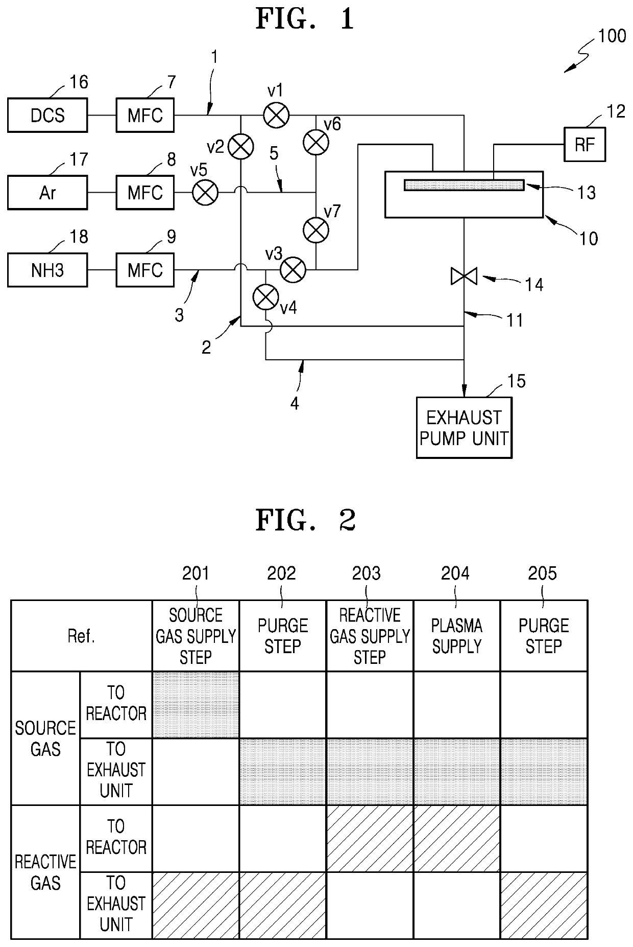
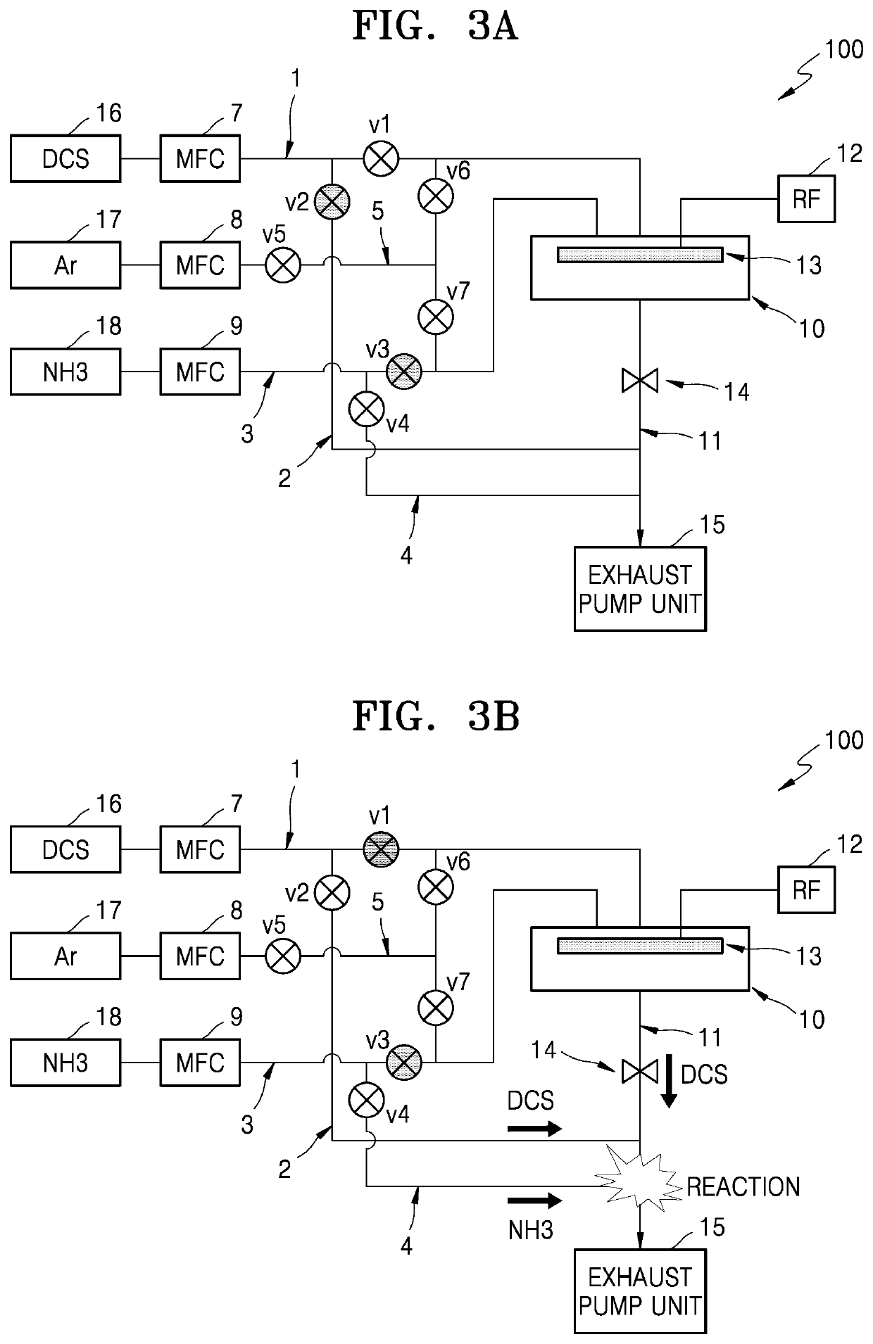
[0036]Reference will now be made in detail to embodiments, examples of which are illustrated in the accompanying drawings, wherein like reference numerals refer to like elements throughout. In this regard, the present embodiments may have different forms and should not be construed as being limited to the descriptions set forth herein. Accordingly, the embodiments are merely described below, by referring to the figures, to explain aspects of the present description.

[0037]Hereinafter, embodiments of the present disclosure will be described in detail with reference to the accompanying drawings.

[0038]Embodiments of the present disclosure are provided to more fully explain the present disclosure to those of ordinary skill in the art, and embodiments set forth herein may be changed in many different forms and are not intended to limit the scope of the present disclosure. Rather, these embodiments are provided so that this disclosure will be thorough and complete, and will fully convey th...


PUM

PropertyMeasurementUnit
Timeaaaaaaaaaa
Timeaaaaaaaaaa
Timeaaaaaaaaaa

Abstract

A thin film forming method includes: a first operation of supplying a source gas at a first flow rate into a reactor; a second operation of purging the source gas in the reactor to an exhaust unit; a third operation of supplying a reactive gas at a second flow rate into the reactor; a fourth operation of supplying plasma into the reactor; and a fifth operation of purging the reactive gas in the reactor to the exhaust unit, wherein, during the second to fifth operations, the source gas is bypassed to the exhaust unit, and a flow rate of the source gas bypassed to the exhaust unit is less than the first flow rate. According to the thin film forming method, the consumption of the source gas and the reactive gas may be reduced, and the generation of reaction by-products in the exhaust unit may be minimized.

Description

CROSS-REFERENCE TO RELATED APPLICATION[0001]This application claims the benefit of U.S. Provisional Application No. 62 / 668,685, filed on May 8, 2018, in the United States Patent and Trademark Office, the disclosure of which is incorporated herein in its entirety by reference.BACKGROUND1. Field[0002]One or more embodiments relate to a thin film forming method and a substrate processing apparatus, and particularly, to a thin film forming method and a substrate processing apparatus, which are capable of reducing the consumption of a source gas and a reactive gas used during a thin film forming process. More particularly, one or more embodiments relate to a method of reducing the consumption of a dichlorosilane (DCS; SiH2Cl2) source in a SiN thin film deposition process using the DCS source.[0003]One or more embodiments also relate to a thin film forming method and a substrate processing apparatus that are capable of preventing the generation of reaction byproducts.2. Description of the...

Claims


Application Information

Patent Timeline
IPC IPC(8): G01F7/00G01F1/78G01F1/40
CPCG01F1/78G01F1/40G01F7/005C23C16/345C23C16/45544C23C16/52H01L21/0217H01L21/02211H01L21/02274H01L21/0228C23C16/45542H01L21/02315H01L21/67017C23C16/45536
Inventor KIM, YOUNGJAEKIM, YOUNGHOON
Owner ASM IP HLDG BV
Why Eureka
Try Eureka