Pixel unit and array substrate comprising the same

a technology of array substrate and pixel unit, which is applied in the field of liquid crystal display, can solve the problems of non-uniform gap of liquid crystal cell, non-uniform etching of metal, and common watermark defect, and achieve the effect of avoiding storage capacitor differen

Active Publication Date: 2019-12-26
TCL CHINA STAR OPTOELECTRONICS TECH CO LTD
View PDF1 Cites 0 Cited by
  • Summary
  • Abstract
  • Description
  • Claims
  • Application Information

AI Technical Summary

Benefits of technology

[0007]Aiming at the technical defect in the prior art, the present disclosure provides a pixel unit. Through arranging a structure of a first electrode and a second electrode of a storage capacitor, storage capacitors of different pixel units can be maintained consistent with one another when an alignment accuracy between the first electrode and the second electrode in one pixel unit is different from that in another pixel unit. In this manner, the watermark resulted from storage capacitor difference can be avoided.

Problems solved by technology

Watermark defect is a commonly seen problem in a liquid crystal display panel.
There are many reasons for the watermark defect, such as non-uniform gap of a liquid crystal cell, non-uniform etching of metal, and alignment accuracy difference among different regions of the panel.
The alignment accuracy difference among different regions of the panel will result in inconsistent storage capacitors of pixel units in different regions of the panel, and thus watermark will be generated.
The difference between the areas of the overlapping regions will result in changing of the storage capacitor.
The alignment accuracy difference among different regions will result in difference among storage capacitors in different regions.
The watermark defect will be generated by the difference among storage capacitors during low gray-scale display, and consequently, display quality of the product will be adversely affected.

Method used


Image

  • Pixel unit and array substrate comprising the same
  • Pixel unit and array substrate comprising the same
  • Pixel unit and array substrate comprising the same

Examples


embodiment 1

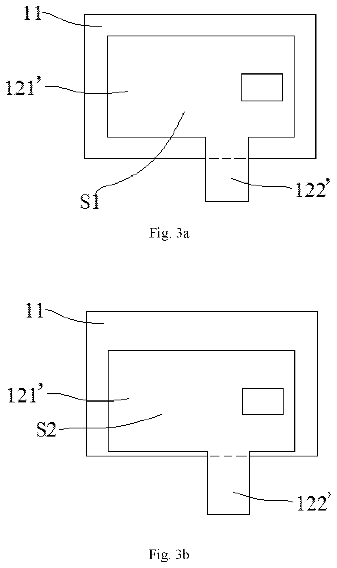
[0036]FIG. 4a schematically shows a structure of a storage capacitor of a pixel unit according to the present embodiment. The storage capacitor of the pixel unit comprises a first electrode 21 arranged on a first metal layer and a second electrode 22 arranged on a second metal layer. At the same time, an insulation layer is arranged between the first electrode 21 and the second electrode 22. FIG. 4a schematically shows the structure of the storage capacitor when observing along a normal line direction of an array substrate. It can be seen from FIG. 4a that, the first electrode 21 comprises a first region 211, and the second electrode 22 comprises a second region 221, a third region 222, and a fourth region 223. During manufacturing of the array substrate, an alignment accuracy between the first electrode 21 and the second electrode 22 in one pixel unit is different from that in another pixel unit. FIG. 4a schematically shows the structure of the storage capacitor when the second ele...

embodiment 2

[0046]FIG. 5 schematically shows a structure of a storage capacitor of a pixel unit according to the present embodiment. Similar to that in embodiment 1, the storage capacitor of the pixel unit comprises a first electrode 31 arranged on a first metal layer and a second electrode 32 arranged on a second metal layer. At the same time, an insulation layer is arranged between the first electrode 31 and the second electrode 32. FIG. 5 schematically shows the structure of the storage capacitor when observing along a normal line direction of an array substrate. It can be seen from FIG. 5 that, the first electrode 31 comprises a first region 311 and a blank region 312, and no metal is arranged in the blank region 312. The second electrode 32 comprises a second region 321 and a third region 322. During manufacturing of the array substrate, an alignment accuracy between the first electrode 31 and the second electrode 32 in one pixel unit is different from that in another pixel unit. FIG. 5 sc...


PUM


Abstract

The technical field of liquid crystal display is related to. A pixel unit is provided. The pixel unit includes a storage capacitor that is arranged on an array substrate. The storage capacitor includes a first electrode arranged on a first metal layer and a second electrode arranged on a second metal layer. An insulation layer is arranged between the first electrode and the second electrode. The second electrode and the first electrode overlap with each other to form a first overlapping region, an area of which does not change if a deviation of the second electrode relative to the first electrode is within a preset distance. Storage capacitor difference among different pixel units generated by alignment accuracy difference thereof can be eliminated, and watermark which would be generated otherwise can be eliminated as well. An array substrate is further provided, which includes the storage capacitor of the aforesaid pixel unit. A quality of a product can be improved.

Description

CROSS REFERENCE TO RELATED APPLICATION[0001]The present application claims priority of Chinese patent application CN201710319935.X, entitled “Pixel Unit and Array Substrate Comprising the Same” and filed on May 9, 2017, the entirety of which is incorporated herein by reference.FIELD OF THE INVENTION[0002]The present disclosure relates to the technical field of liquid crystal display, and particularly to a pixel unit and an array substarte comprising the same.BACKGROUND OF THE INVENTION[0003]Watermark defect is a commonly seen problem in a liquid crystal display panel. In general, non-uniform images, such as raindrop-shaped defect, cluster-shaped defect, and fog-shaped defect are all called as watermark defect. There are many reasons for the watermark defect, such as non-uniform gap of a liquid crystal cell, non-uniform etching of metal, and alignment accuracy difference among different regions of the panel. The alignment accuracy difference among different regions of the panel will ...

Claims


Application Information

Patent Timeline
Patent Type & Authority Applications(United States)
IPC IPC(8): H01L49/02H01L27/12
CPCH01L27/1255H01L28/60G09G3/36H01L27/124H10K59/1216
Inventor AN, LIYANG
Owner TCL CHINA STAR OPTOELECTRONICS TECH CO LTD
Why Eureka
Try Eureka