Metamaterial waveguides and shielded bridges for quantum circuits

a technology of shielded bridges and waveguides, applied in waveguides, quantum computers, instruments, etc., can solve problems such as limiting the scalability of quantum processors

Active Publication Date: 2020-02-13
CALIFORNIA INST OF TECH
View PDF0 Cites 16 Cited by
  • Summary
  • Abstract
  • Description
  • Claims
  • Application Information

AI Technical Summary

Benefits of technology

[0014]In some embodiments a method of forming a shielded bridge for a coplanar waveguide (CPW) comprises depositing one or more first electron beam (e-beam) resist layers on a dielectric substrate and performing 3-D grayscale lithography on the one or more first e-beam resist layers to create removable portions and a tenacious portion of the one or more first e-beam resist layers. The removable portions of the one or more first e-beam resist layers are removed such that the tenacious portion of the one or more first e-beam resist layers remains and extends between a first termination region and a second termination region. A first layer of metal is deposited to form a ground bridge that extends from the first termination region, across the tenacious portion of the one or more first e-beam resist layers, to the second termination region, such that the ground bridge is electrically coupled to the first and second termination regions. One or more second e-beam resist layers are deposited on the dielectric substrate and 3-D grayscale lithography is performed on the one or more second e-beam resist layers to create removable regions and a tenacious region of the one or more second e-beam resist layers. The removable regions of the one or more second e-beam resist layers are removed such that the tenacious region of the one or more second e-beam resist layers remains and extends between a first terminal and a second terminal of the CPW. A second layer of metal is deposited to form a signal bridge that extends from the first terminal of the CPW, across the tenacious region of the one or more second e-beam resist layers to the second terminal of the CPW such that the signal bridge is electrically coupled to the first and second terminals of the CPW and all remaining portions of the one or more second e-beam resist layers are removed.
[0015]In some embodiments a reflow of the tenacious portion of one or more first e-beam resist layers is performed before depositing the first layer of metal. In various embodiments a reflow of the tenacious region of the one or more second e-beam resist layers is performed before depositing the second layer of metal.

Problems solved by technology

As the number of qubits in a quantum processor is increased, these characteristics result in complex interconnect and routing schemes that limit scalability of the quantum processor.

Method used


Image

  • Metamaterial waveguides and shielded bridges for quantum circuits
  • Metamaterial waveguides and shielded bridges for quantum circuits
  • Metamaterial waveguides and shielded bridges for quantum circuits

Examples


Embodiment Construction

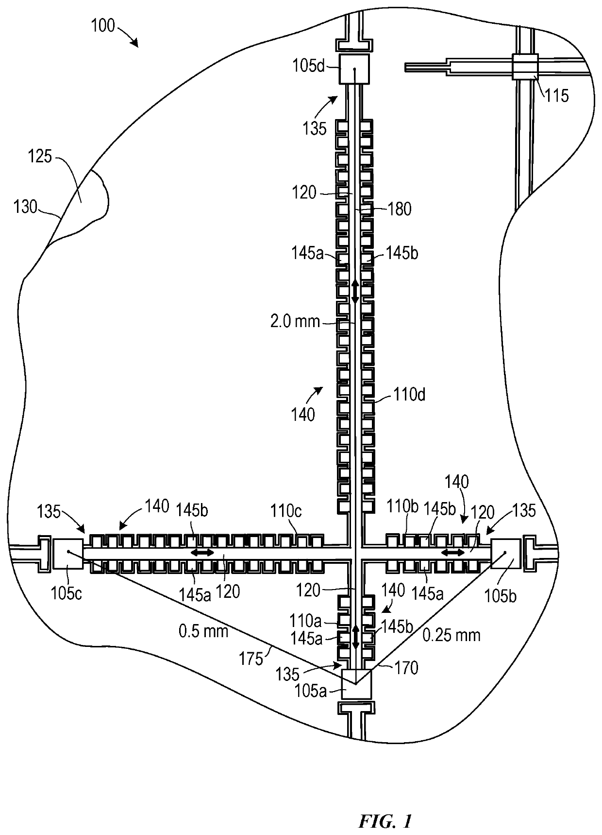
[0034]The present invention relates generally to methods and systems for quantum computing. More specifically, the present invention relates to methods and systems for quantum communications and qubit interconnect structures enabling increased scalability of quantum computing systems.

[0035]In order to better appreciate the features and aspects of the present disclosure, further context for the disclosure is provided in the following section by discussing one particular implementation of a quantum computing system that includes metamaterial waveguides and shielded bridges according to embodiments of the disclosure. These embodiments are for explanatory purposes only and other embodiments may be employed in other configurations. For example, embodiments of the disclosure can also be used to couple coplanar waveguide structures to qubits.

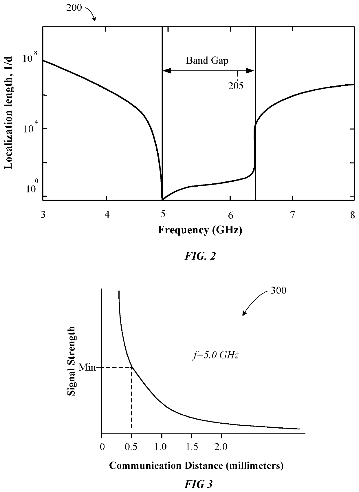
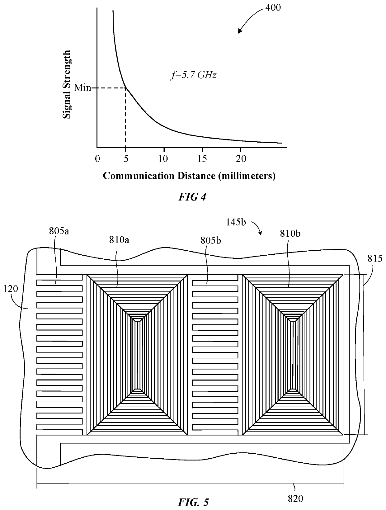
[0036]Some embodiments of the present disclosure relate to metamaterial waveguides that are used to communicatively couple one or more qubits on a “qu...


PUM


Abstract

Metamaterial waveguides and shielded bridges are employed to improve the scalability and routing of quantum computing circuits. A metamaterial waveguide includes a signal conductor that has a periodic array of lumped element resonators distributed along and electrically coupled to a signal conductor. The periodic array of lumped element resonator pairs defines a bandgap within an operating bandwidth of the waveguide. Qubits can communicate within the operating bandwidth of the waveguide and communications via the waveguide can be controlled by changing a center frequency of the qubits. A shielded bridge is used to cross over high frequency communications and control CPW's in a quantum computing circuit. The shielded bridge includes a signal bridge that is elevated and extends over a separate CPW, and a ground bridge positioned between the signal bridge and the separate CPW.

Description

CROSS-REFERENCES TO RELATED APPLICATIONS[0001]This application claims priority to U.S. Provisional Patent Application No. 62 / 652,765, filed on Apr. 4, 2018, entitled “Compact, Low Loss, Low Disorder, Microwave Metamaterials for Superconducting Quantum Circuits” and to U.S. Provisional Patent Application No. 62 / 638,755, filed on Mar. 5, 2018, entitled “Hopovers: Airbridges for Reduced Crosstalk in Superconducting Circuits”, the disclosures of which are hereby incorporated by reference in their entirety for all purposes.[0002]The following regular U.S. patent applications (including this one) are being filed concurrently, and the entire disclosure of the other applications are incorporated by reference into this application for all purposes:[0003]Application Ser. No. ______, filed Mar. 5, 2019, entitled “TECHNIQUES FOR TRANSDUCTION AND STORAGE OF QUANTUM LEVEL SIGNALS” (Attorney Docket No. 086544-1125985 (022410US));[0004]Application Ser. No. ______, filed Mar. 5, 2019, entitled “TECH...

Claims


Application Information

Patent Timeline
Patent Type & Authority Applications(United States)
IPC IPC(8): H01P3/00G06N10/00
CPCG06N10/00G02F2202/30H01P3/00H01P1/2005H01P1/20381
Inventor PAINTER, OSKARMIRHOSSEINI NIRI, SEYED MOHAMMADKIM, EUN JONGSIPAHIGIL, ALPFERREIRA, VINICIUS THADDEU DOS SANTOSKELLER, ANDREW J.KALAEE, MAHMOUDFANG, MICHAEL T.
Owner CALIFORNIA INST OF TECH
Why Eureka
Try Eureka