Semiconductor structure and method for forming same

a technology of semiconductors and structures, applied in the direction of semiconductor devices, electrical equipment, transistors, etc., can solve the problems of deteriorating the channel control capability of the gate, achieve the effect of improving the channel control capability of the subsequently formed gate structure, alleviating the short-channel effect of the device, and reducing the cost of production

Active Publication Date: 2020-02-20
SEMICONDUCTOR MANUFACTURING INTERNATIONAL (BEIJING) CORP +1
View PDF1 Cites 9 Cited by
  • Summary
  • Abstract
  • Description
  • Claims
  • Application Information

AI Technical Summary

Benefits of technology

[0010]In embodiments and implementations of the present disclosure, a channel structure layer is formed on fins, where the channel structure layer includes a first channel structure layer located on at least one fin and a second channel structure layer located on at least one fin. The first channel structure layer includes multiple channel laminates, each channel laminate includes a first sacrificial layer and a first channel layer located on the first sacrificial layer, and the second channel structure layer is a second channel layer of a single-layer structure. The first channel structure layer is formed, so that a channel controlling capability of the subsequently formed gate structure can be improved, thereby alleviating short-channel effects of a device. The second channel structure layer is formed, so that a self-heating effect of the device can be alleviated. In summary, by integrating a GAA transistor and a fin-type field effect transistor into one device unit area, embodiments and implementations of the present disclosure alleviate the self-heating effect while improving the channel controlling capability of the gate structure, so that overall performance of the device can be improved.
[0011]In some implementations, the channel structure layer further includes a third channel structure layer located on at least one fin. The third channel structure layer includes a third channel layer, a second sacrificial layer located on the third channel layer, and a fourth channel layer located on the second sacrificial layer. By using the third channel structure, the formed device has properties of both the GAA transistor and the fin-type field effect transistor, so that the short-channel effects and the self-heating effect of the device can be further balanced, thereby further improving the overall performance of the device.

Problems solved by technology

Therefore, a channel controlling capability of the gate is deteriorated.

Method used


Image

  • Semiconductor structure and method for forming same
  • Semiconductor structure and method for forming same
  • Semiconductor structure and method for forming same

Examples


Embodiment Construction

[0015]It can be learned from the background art that it is desirable to improve a performance of current GAA transistors. Discussed below are reasons why a device performance of GAA transistors still need to be improved is analyzed with reference to a semiconductor structure.

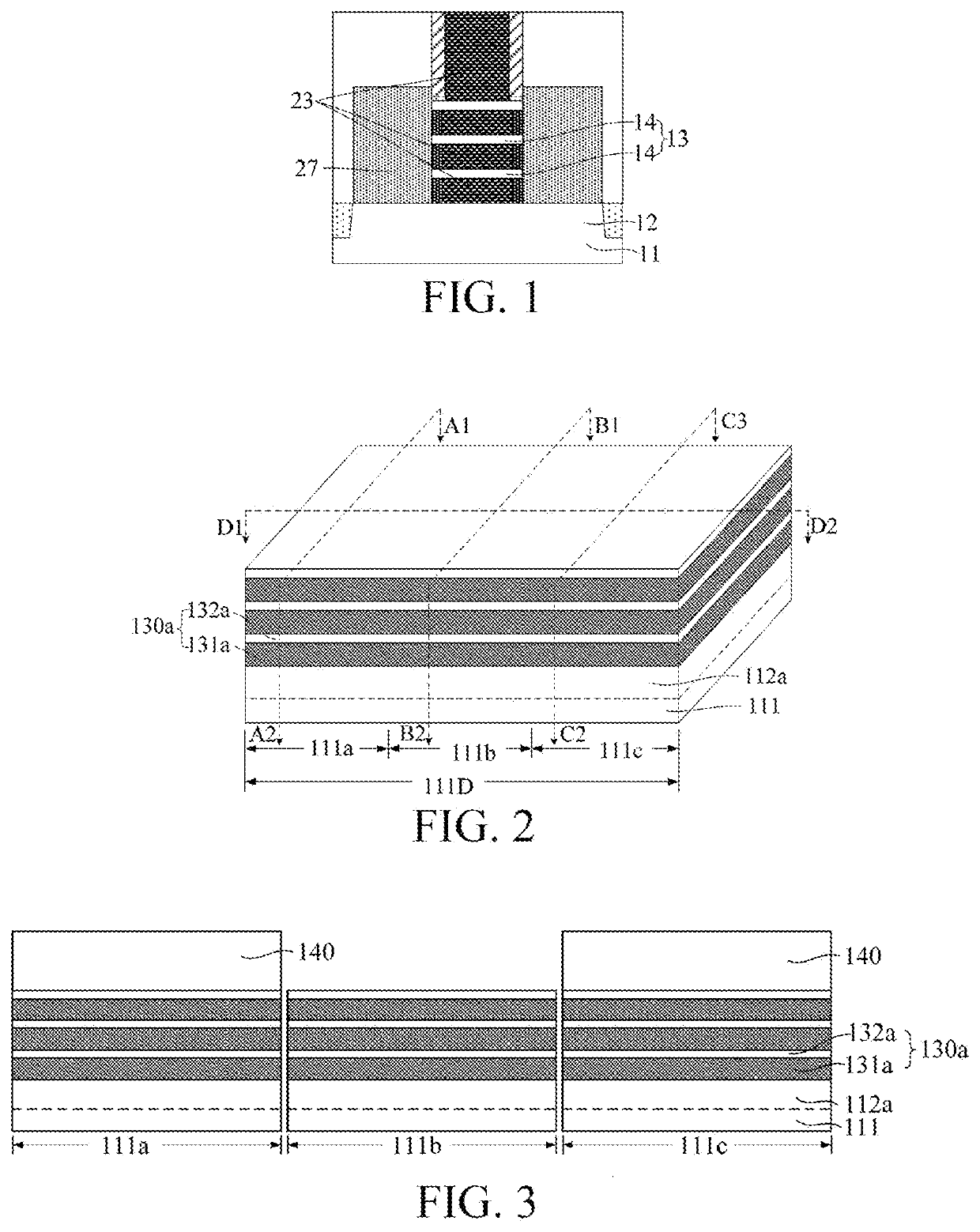
[0016]Referring to FIG. 1, FIG. 1 shows a schematic structural diagram of a semiconductor structure.

[0017]The semiconductor structure includes: a substrate 11; a fin 12 protruding from the surface of the substrate 11; a channel structure 13, located on the fin 12 and spaced apart from the fin 12, where the channel structure 13 includes multiple channel layers 14 spaced apart; a gate structure 23 across the channel structure 13, where the gate structure 23 covers a part of the top of the fin 12 and surrounds the channel layers 14; and a source-drain doping layer 27, located in the channel structure 13 on two sides of the gate structure 23 and in contact with the fin 12.

[0018]Compared with a fin-type field effect ...


PUM

PropertyMeasurementUnit
relative dielectric constantaaaaaaaaaa
semiconductor structureaaaaaaaaaa

Abstract

A semiconductor structure and a method for forming same are provided. One form of the method includes: providing a substrate including a device unit area, where at least two fins are formed on the substrate of the device unit area, a channel structure layer is formed on the fins, the channel structure layer includes a first channel structure layer located on at least one fin and a second channel structure layer located on at least one fin, the first channel structure layer includes multiple channel laminates, each channel laminate includes a first sacrificial layer and a first channel layer located on the first sacrificial layer, and the second channel structure layer is a second channel layer of a single-layer structure; forming a dummy gate structure across the channel structure layer of the device unit area; forming a source-drain doping layer in the channel structure layer on two sides of the dummy gate structure; forming an interlayer dielectric layer on the substrate exposed by the dummy gate structure; and after forming the interlayer dielectric layer, forming a gate structure at positions of the dummy gate structure and the first sacrificial layer. The present disclosure can improve overall performance of a device.

Description

RELATED APPLICATIONS[0001]The present application claims priority to Chinese Patent Appln. No. 201810920760.2, filed Aug. 14, 2018, the entire disclosure of which is hereby incorporated by reference.BACKGROUNDTechnical Field[0002]Embodiments and implementations of the present disclosure relate to the field of semiconductor manufacturing, and in particular, to a semiconductor structure and a method for forming same.Related Art[0003]With the rapid development of semiconductor manufacturing technology, semiconductor devices are developed to have a higher element density and a higher integration level. Semiconductor process nodes are continually becoming smaller following the development trend of the Moore's law. Transistors are widely applied and are currently the most fundamental semiconductor devices. Therefore, as the element density and the integration level of the semiconductor devices are improved, a channel length of transistors has to be reduced to adapt to the smaller process ...

Claims


Application Information

Patent Timeline
Patent Type & Authority Applications(United States)
IPC IPC(8): H01L29/786H01L29/78H01L29/423H01L29/66H01L21/02
CPCH01L29/785H01L29/66545H01L29/78696H01L21/02636H01L29/42392H01L29/66795H01L29/0657H01L29/0684H01L27/0886H01L21/823431H01L29/66772H01L29/78684
Inventor WANG, NAN
Owner SEMICONDUCTOR MANUFACTURING INTERNATIONAL (BEIJING) CORP
Why Eureka
Try Eureka