Supercharge Your Innovation With Domain-Expert AI Agents!

Method Of Reducing Lift-Off Related Redeposit Defects On Semiconductor Wafers

a technology of semiconductor wafers and defects, applied in the field of semiconductor wafer processing, can solve the problems of difficult removal and impact on the yield of final acceptable devices

Active Publication Date: 2020-03-05
II VI DELAWARE INC
View PDF0 Cites 0 Cited by
  • Summary
  • Abstract
  • Description
  • Claims
  • Application Information

AI Technical Summary

Benefits of technology

The patent text describes a method for manufacturing a semiconductor device using a lift-off process. The method includes steps of forming a layer of photoresist, patterning the layer of photoresist, depositing a metal contact layer, and exposing the metal contact layer to a plasma treatment. The plasma treatment creates a hydrophilic surface on the metal contact layer, which reduces the likelihood of the metal adhering to the substrate and forming unwanted redeposits. The method also helps remove organic contaminants from the structure. The technical effect of the patent text is to improve the efficiency and reliability of the semiconductor device manufacturing process.

Problems solved by technology

These redeposits form temporary bonds with the wafer surface and are difficult to remove, even by performing a second lift-off process.
As a result, any of the individual die on a given wafer that are found to include these redeposits must be discarded, impacting the yield of the final acceptable devices.

Method used


Image

  • Method Of Reducing Lift-Off Related Redeposit Defects On Semiconductor Wafers
  • Method Of Reducing Lift-Off Related Redeposit Defects On Semiconductor Wafers
  • Method Of Reducing Lift-Off Related Redeposit Defects On Semiconductor Wafers

Examples


Embodiment Construction

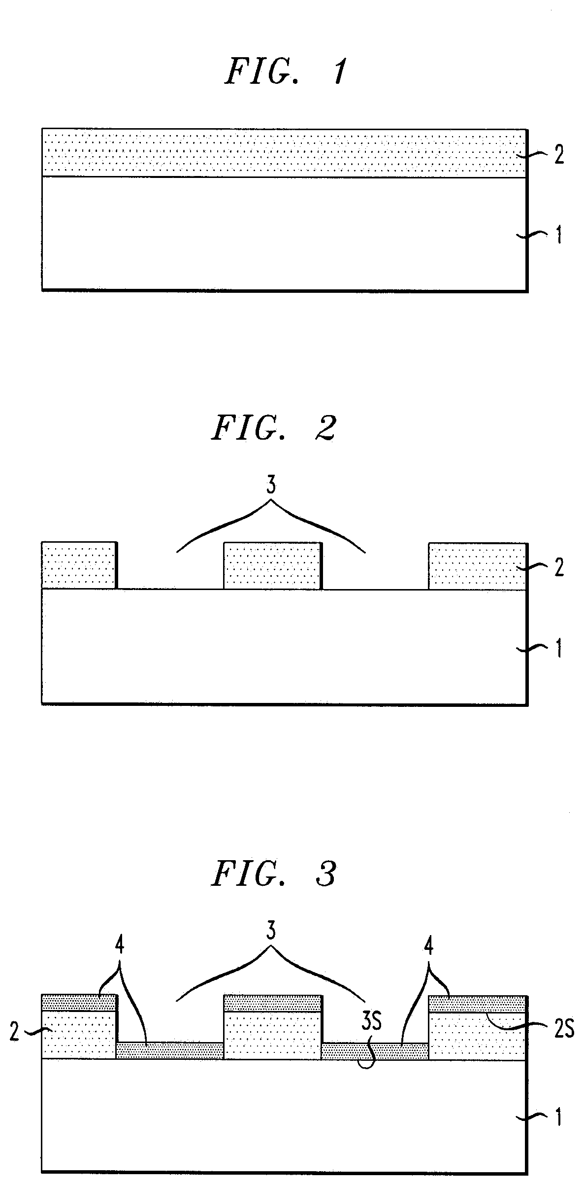
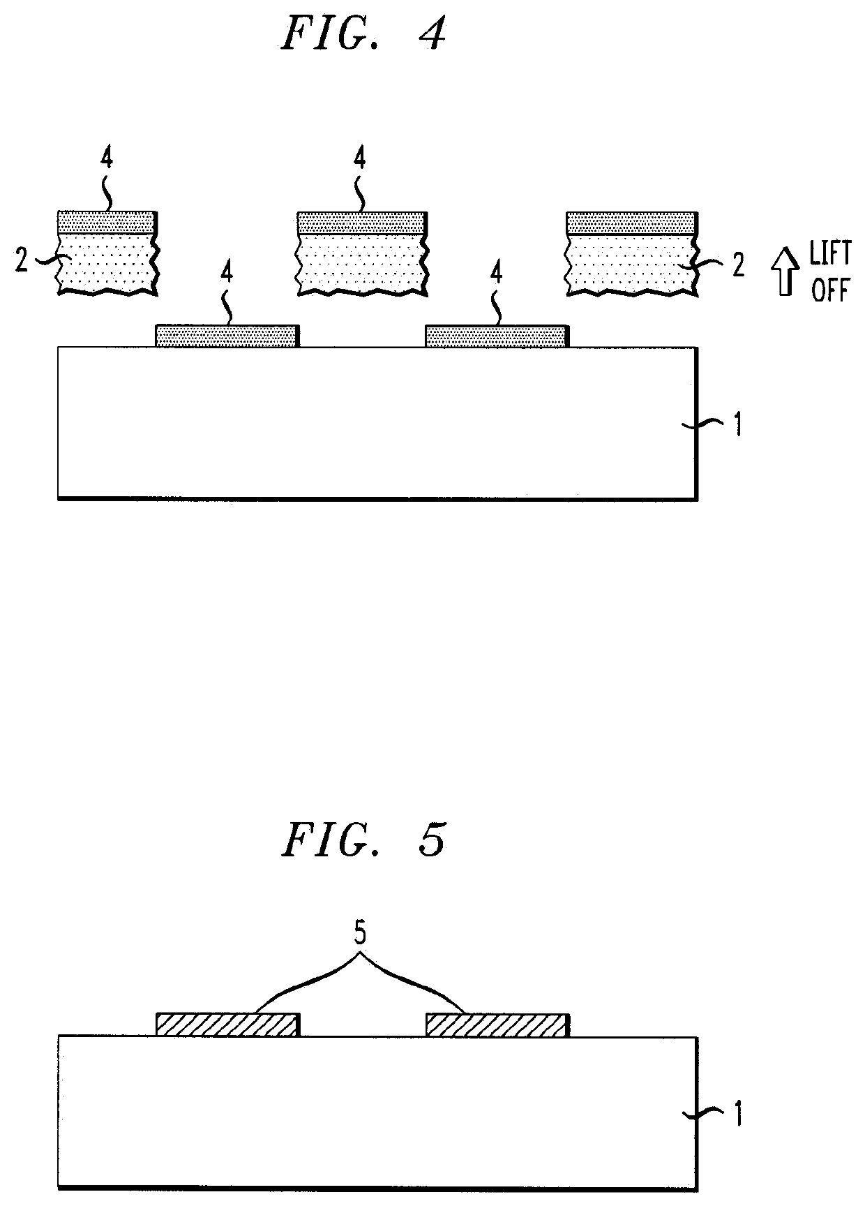
[0016]As mentioned above, lift-off is a technique used in some semiconductor fabrication processes to create a patterned layer of target material (for example, metal) on a wafer structure. FIGS. 1-5 illustrate a set of typical prior art process steps used in performing a typical lift-off technique. FIG. 1 illustrates a starting material for the process, in the form of a substrate 1 that has presumably been processed to include various semiconductor devices / regions (not specifically shown). To begin the formation of a metal contact structure using a lift-off process, substrate 1 is initially covered with a photoresist material 2. Photoresist material 2 is subsequently patterned, using well-known techniques, to expose regions 3 where it is desired to form the layer of target material. This step in the process is shown in FIG. 2.

[0017]Once patterned, a layer 4 of the target material is deposited (perhaps using an evaporation process, for example) to coat the top surface of the structur...


PUM

PropertyMeasurementUnit
pressureaaaaaaaaaa
pressureaaaaaaaaaa
contact angleaaaaaaaaaa

Abstract

A plasma treatment is utilized prior to a conventional lift-off process to increase the hydrophilic characteristics of the surface of the sacrificial metal over the photoresist and minimize its ability to redeposit on the wafer surface. Highly-energized atoms (or molecules) in the plasma interact with the surface atoms of the metal, creating a temporary hydrophilic condition at the surface. This increased wettability of the metal layer surface thus minimizes the probability that subsequently removed thin film metal will be able to bond with the wafer surface. The metal layer may comprise a typical stack of Ti / Pt / Au, and the plasma treatment may use an O2-based plasma or a CF4-based plasma, among others.

Description

TECHNICAL FIELD[0001]The present invention relates to semiconductor wafer processing and, more particularly, to a method of reducing the redeposit of metallic contact material during a lift-off process.BACKGROUND OF THE INVENTION[0002]In the process of forming a thin film metal contact using a conventional lift-off technique, it is typical for some portions of the “lifted off” material film to redeposit on the wafer surface. These redeposits form temporary bonds with the wafer surface and are difficult to remove, even by performing a second lift-off process. As a result, any of the individual die on a given wafer that are found to include these redeposits must be discarded, impacting the yield of the final acceptable devices.SUMMARY OF THE INVENTION[0003]The present invention relates to the inclusion of an additional step in the conventional lift-off process that (temporarily) makes the metal's surface hydrophilic and thus reduces the probability that any portions of the removed met...

Claims


Application Information

Patent Timeline
Patent Type & Authority Applications(United States)
IPC IPC(8): H01L21/027H01L21/02
CPCH01L21/02252H01L21/0273H01L21/022H01L21/02112H01S5/423H01L21/0272H01L21/321H01S5/04252H01S5/18394
Inventor KANUKUNTLA, PALLAVRAMPERSAD, ASHAMIN
Owner II VI DELAWARE INC
Features
  • R&D
  • Intellectual Property
  • Life Sciences
  • Materials
  • Tech Scout
  • Unparalleled Data Quality
  • Higher Quality Content
  • 60% Fewer Hallucinations
Learn More