Supercharge Your Innovation With Domain-Expert AI Agents!

Semiconductor package assembly and method for forming the same

a technology of semiconductor package and assembly method, which is applied in the direction of semiconductor/solid-state device details, semiconductor devices, electrical apparatus, etc., can solve the problems of increasing the cost of manufacturing these semiconductor package assemblies, many different sizes of memory dies on the market,

Active Publication Date: 2020-03-05
MEDIATEK INC
View PDF0 Cites 2 Cited by
  • Summary
  • Abstract
  • Description
  • Claims
  • Application Information

AI Technical Summary

Benefits of technology

This approach allows for the use of the same semiconductor package assembly layout across different memory die sizes, reducing manufacturing costs and preventing reliability issues associated with warpage, while ensuring electrical connections remain effective.

Problems solved by technology

However, a problem with such a semiconductor package assembly is that there are so many different sizes of memory dies on the market.
It is necessary to design different layouts for semiconductor package assemblies using memory dies of different sizes, and this can lead to the rising cost of manufacturing these semiconductor package assemblies.

Method used


Image

  • Semiconductor package assembly and method for forming the same
  • Semiconductor package assembly and method for forming the same
  • Semiconductor package assembly and method for forming the same

Examples


Embodiment Construction

[0022]The following description is of the best-contemplated mode of carrying out the invention. This description is made for the purpose of illustrating the general principles of the invention and should not be taken in a limiting sense. The scope of the invention is determined by reference to the appended claims.

[0023]The present invention will be described with respect to particular embodiments and with reference to certain drawings, but the invention is not limited thereto and is only limited by the claims. The drawings described are only schematic and are non-limiting. In the drawings, the size of some of the elements may be exaggerated for illustrative purposes and not drawn to scale. The dimensions and the relative dimensions do not correspond to actual dimensions in the practice of the invention.

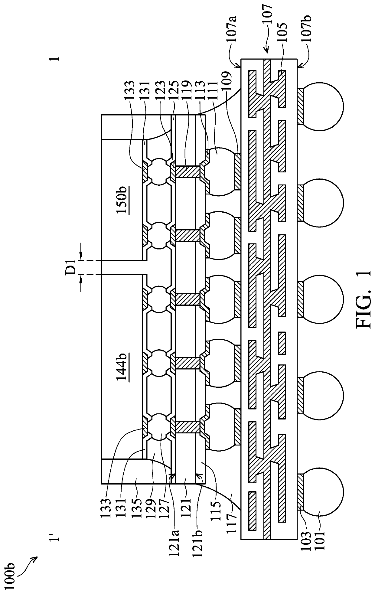
[0024]FIG. 1 is a cross-sectional view of a semiconductor package assembly 100b, in accordance with some embodiments of the disclosure. Additional features can be added to the semicon...


PUM


Abstract

A semiconductor package assembly and method for forming the same are provided. The semiconductor package assembly includes a first semiconductor die and a second semiconductor die disposed on a first surface of a substrate. The first semiconductor die includes a peripheral region having a second edge facing the first edge of the second semiconductor die and a third edge opposite to the second edge, a circuit region surrounded by the peripheral region, wherein the circuit region has a fourth edge adjacent to the second edge and a fifth edge adjacent to the third edge. A minimum distance between the second edge and the fourth edge is a first distance, a minimum distance between the third edge and the fifth edge is a second distance, and the first distance is different from the second distance.

Description

CROSS REFERENCE TO RELATED APPLICATIONS[0001]This application is a Continuation application of pending U.S. application Ser. No. 16 / 043,326, filed on Jul. 24, 2018, which claims the benefit of U.S. Provisional Application No. 62 / 541,199 filed on Aug. 4, 2017 and U.S. Provisional Application No. 62 / 549,015 filed on Aug. 23, 2017, the entirety of which are incorporated by reference herein.BACKGROUND OF THE INVENTIONField of the Invention[0002]The present invention relates to a semiconductor package assembly, and in particular to a semiconductor package assembly with horizontally discrete semiconductor dies and memory dies.Description of the Related Art[0003]A semiconductor package assembly can not only provide a semiconductor die with protection from environmental contaminants, but it can also provide an electrical connection between the semiconductor die packaged therein and a substrate, such as a printed circuit board (PCB). For instance, a semiconductor die may be enclosed in an en...

Claims


Application Information

Patent Timeline
Patent Type & Authority Applications(United States)
IPC IPC(8): H01L25/18H01L21/78H01L25/00H01L23/00H01L25/065
CPCH01L21/78H01L2924/15311H01L24/48H01L2224/16235H01L2224/49175H01L24/13H01L24/16H01L2224/32225H01L2224/48227H01L25/50H01L2924/1432H01L2224/32137H01L2924/1436H01L2924/1431H01L24/32H01L2224/48011H01L2224/16227H01L2224/49176H01L24/49H01L25/18H01L25/0655H01L24/29H01L2224/32106H01L23/5384H01L23/3128H01L21/56H01L24/02H01L24/11H01L2224/02331H01L2224/111H01L2224/13008H01L2224/73204H01L2224/16225H01L2924/18161H01L23/562H01L2224/131H01L2224/291H01L2924/00H01L2924/014
Inventor CHANGPENG, I-HSUANLIN, TZU-HUNG
Owner MEDIATEK INC
Features
  • R&D
  • Intellectual Property
  • Life Sciences
  • Materials
  • Tech Scout
  • Unparalleled Data Quality
  • Higher Quality Content
  • 60% Fewer Hallucinations
Learn More