Method for characterisation by cd-sem scanning electronic microscopy

haracterisation technology, applied in the field of implementing a scanning electron microscopy (sem) characterisation technique, can solve the problems of not very reliable measurements of objects of less than 100 nm size, cd-sem techniques give not very reliable measurements, and the empirical threshold applied to any type of pattern is all the less satisfactory

Active Publication Date: 2020-03-19
COMMISSARIAT A LENERGIE ATOMIQUE ET AUX ENERGIES ALTERNATIVES
View PDF1 Cites 0 Cited by
  • Summary
  • Abstract
  • Description
  • Claims
  • Application Information

AI Technical Summary

Benefits of technology

[0037]Taking into account the positions scanned by the beam before arriving at the position Pi makes it possible to introduce the notion of causality into the second theoretical model. Thanks to the given convolution kernel, which contains a temporal dispersion function and a spatial dispersion function, temporal charging effects are taken into account. The effect at the position Pi of the charge deposited at the position Pj depends on the distance between the two positions but also on the time that has gone by between the passage of the primary electron beam in Pj and the passage in Pi.
[0038]For example, if the temporal difference between the instant tj at which the charge has been deposited at the position Pj and the instant ti at which the beam is found at the position Pi is much greater than the characteristic time of charge dissipation mechanisms, the second theoretical model does not take into account the effect of the charge at the position Pj.

Problems solved by technology

The reliable measurement of this critical dimension is today one of the main issues for scanning electron microscopy.
But one of the major problems is the interpretation of the images by thresholding algorithms: it is in fact the choice of this threshold that is going to determine the value of the characteristic size, or critical dimension, of interest.
At present it is known that CD-SEM techniques give not very reliable measurements for objects of size less than 100 nm (difference to reality from a nanometre to several nanometres).
A fixed empirical threshold applied to any type of pattern is all the less satisfactory as there is no direct physical link between the percentage of collected secondary electrons and the real height of the pattern at which it is sought to determine the critical dimension.
Performing these very complex simulations requires great computing power and very long execution times. These characteristics make Monte Carlo type physical simulations generally not very accessible and very little suited to the processing of a large number of CD-SEM images.
One of the major limitations of these techniques is in their incapacity to take into account and to reproduce certain artefacts observed on CD-SEM images.
It may be remarked that the parametric profiles method only takes account of a modelling of profiles along the direction perpendicular to the edges and is thus not able to reproduce the effects of black trails present in the extension of the edges themselves.
In addition, the parametric profiles method does not take into account effects linked to the accumulation of electric charges deposited by the primary electron beam during scanning.
Furthermore, the electron charging of the material during exposure to the primary electron beam is not constant over time.
The temporal dependency of the charging phenomena complicates the processing of the CD-SEM images for the elimination of these artefacts.

Method used


Image

  • Method for characterisation by cd-sem scanning electronic microscopy
  • Method for characterisation by cd-sem scanning electronic microscopy
  • Method for characterisation by cd-sem scanning electronic microscopy

Examples


Embodiment Construction

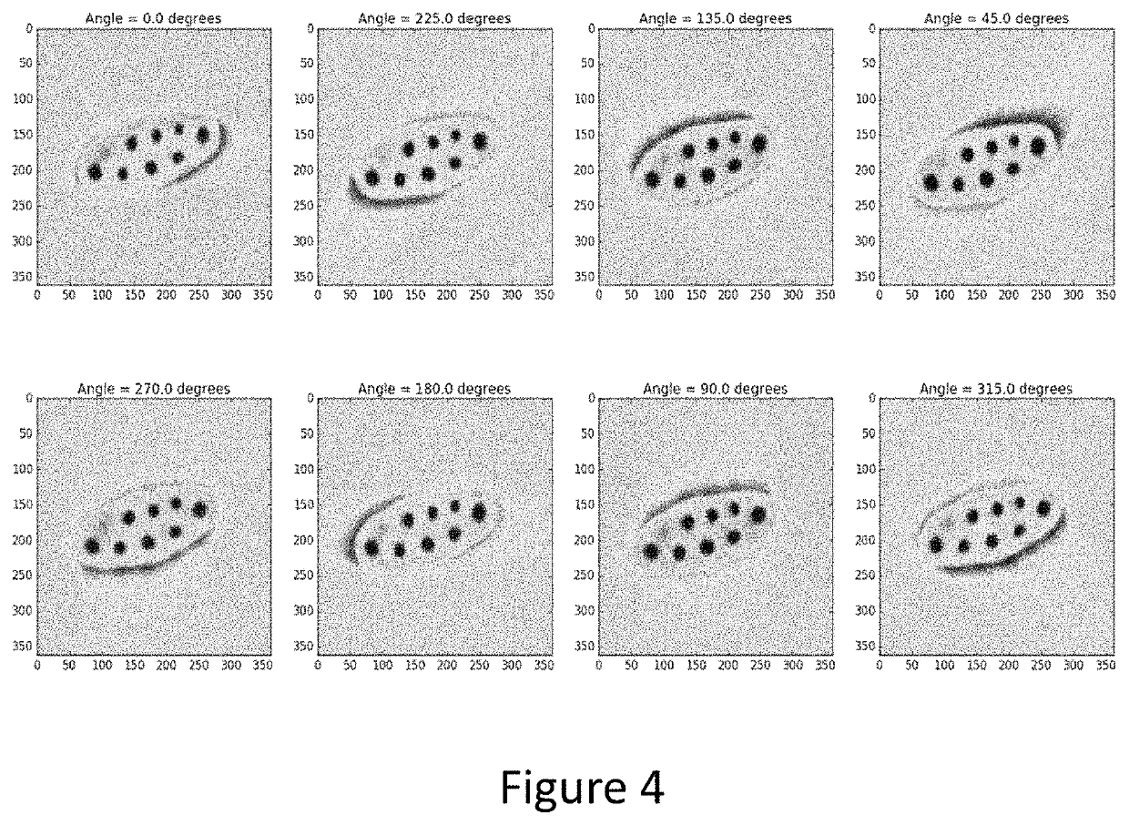
[0076]FIG. 4 shows a series of CD-SEM images taken on a same sample. Each image has been acquired by scanning the surface of the sample according to a different angle. It is obvious that by varying the scanning angle, the images obtained change. This clearly shows that the path of the beam has an influence on the image formation process: the signal measured at a given position on the sample changes according to the path followed by the primary electron beam.

[0077]These observations may be explained by evoking the charging effects described above, including temporal effects.

[0078]It appears necessary to model the signal measured at a given position on the surface of the sample while taking into account the positions scanned by the primary electron beam before arriving at the given position.

[0079]When the incident beam of primary electrons is advancing at the point r on the sample, secondary electrons are generated with an efficiency ρ(r). This efficiency is linked to the nature of th...


PUM

PropertyMeasurementUnit
sizeaaaaaaaaaa
scanning electron microscopyaaaaaaaaaa
critical dimensionaaaaaaaaaa

Abstract

A method for implementing a scanning electron microscopy characterisation technique for the determination of at least one critical dimension of the structure of a sample in the field of dimensional metrology, known as CD-SEM technique, includes producing an experimental image; from a first theoretical model based on parametric mathematical functions, calculating a second theoretical model U(Pi,ti) describing the signal measured at the position Pi at the instant ti, the second model U(Pi,ti) being obtained by algebraic summation of a corrective term S(Pi,ti); determining the set of parameters present in the second theoretical model; wherein the corrective term S(Pi,ti) is calculated by summing the signal coming from the electric charges deposited by the primary electron beam at a plurality of instants t less than or equal to ti.

Description

FIELD OF THE INVENTION[0001]The field of the invention relates to a method for implementing a scanning electron microscopy (SEM) characterisation technique. To this end, the invention pertains to applications in dimensional metrology notably for the semiconductor industry. The field of the invention also relates to the determination of a critical dimension (Critical Dimension Scanning Electron Microscopy or CD-SEM) of the topography of a sample of semiconductors, for example a printed circuit in microelectronicsPRIOR ART[0002]The characterisation of structures of micrometric or nanometric size is today of vital importance in the semiconductor industry, notably in microelectronics, and more generally in the nanotechnologies field. If the case of microelectronics is considered, the precise and reliable measurement of the characteristic dimensions of nanostructures is necessary throughout the different steps of the production process, from the research and development phase up to the p...

Claims


Application Information

Patent Timeline
Patent Type & Authority Applications(United States)
IPC IPC(8): G01N23/2251
CPCG01N2223/401G01N2223/418G01N23/2251G01N2223/611G03F7/70625H01J2237/24578H01J2237/2817H01J2237/2816
Inventor QUEMERE, PATRICKHAZART, JÉRÔME
Owner COMMISSARIAT A LENERGIE ATOMIQUE ET AUX ENERGIES ALTERNATIVES
Why Eureka
Try Eureka