X-ray zoom lens for small angle x-ray scatterometry

a zoom lens and x-ray scatterometry technology, applied in the field of xray metrology systems and methods, can solve the problems of difficult optical radiation penetration to the bottom layer, difficult characterization, and more difficult characterization, and achieve the effect of highest achievable illumination photon flux

Active Publication Date: 2020-12-08
KLA CORP
View PDF55 Cites 1 Cited by
  • Summary
  • Abstract
  • Description
  • Claims
  • Application Information

AI Technical Summary

Benefits of technology

[0019]For a given beam divergence and brightness of the illumination source, the highest achievable photon flux through targets of different size and shape is provided by variation of magnification and the source size and shape. In some embodiments, the illumination source size is controlled to maintain constant illumination beam spot size at the specimen over a wide range of optical magnifications. In some other embodiments, the illumination source size and optical magnification are controlled to adjust the illumination beam spot size at the specimen to match the available measurement area associated with a particular metrology target and to provide the highest achievable illumination photon flux.

Problems solved by technology

As devices (e.g., logic and memory devices) move toward smaller nanometer-scale dimensions, characterization becomes more difficult.
Devices incorporating complex three-dimensional geometry and materials with diverse physical properties contribute to characterization difficulty.
For example, modern memory structures are often high-aspect ratio, three-dimensional structures that make it difficult for optical radiation to penetrate to the bottom layers.
Optical metrology tools utilizing infrared to visible light can penetrate many layers of translucent materials, but longer wavelengths that provide good depth of penetration do not provide sufficient sensitivity to small anomalies.
As a result, the parameters characterizing the target often cannot be reliably decoupled with available measurements.
However, the mirror like structure of 3D FLASH intrinsically causes decreasing light intensity as the illumination propagates deeper into the film stack.
This causes sensitivity loss and correlation issues at depth.
Optical radiation is often unable to penetrate layers constructed of these materials.
As a result, measurements with thin-film scatterometry tools such as ellipsometers or reflectometers are becoming increasingly challenging.
However, these approaches have not reliably overcome fundamental challenges associated with measurement of many advanced targets (e.g., complex 3D structures, structures smaller than 10 nm, structures employing opaque materials) and measurement applications (e.g., line edge roughness and line width roughness measurements).
Atomic force microscopes (AFM) and scanning-tunneling microscopes (S™) are able to achieve atomic resolution, but they can only probe the surface of the specimen.
In addition, AFM and S™ microscopes require long scanning times. Scanning electron microscopes (SEM) achieve intermediate resolution levels, but are unable to penetrate structures to sufficient depth.
Thus, high-aspect ratio holes are not characterized well.
In addition, the required charging of the specimen has an adverse effect on imaging performance.
X-ray reflectometers also suffer from penetration issues that limit their effectiveness when measuring high aspect ratio structures.
For example, transmission electron microscopes (TEM) achieve high resolution levels and are able to probe arbitrary depths, but TEM requires destructive sectioning of the specimen.
But, these techniques require sample destruction and lengthy process times. The complexity and time to complete these types of measurements introduces large inaccuracies due to drift of etching and metrology steps.
In addition, these techniques require numerous iterations which introduce registration errors.
However, imaging a finite sized x-ray source onto the wafer under measurement remains challenging, particularly for small metrology targets and metrology targets of varying size.
A critical challenge is to enable variable magnification to accommodate different sized metrology targets, while maximizing photon flux through the target.
The need to replace optics and related hardware every time a different magnification is required is impractical in a semiconductor fabrication setting.
The need to physically relocate optics, source, and sample with respect to one another is highly undesirable in a semiconductor fabrication setting.
However, this approach comes at a cost of reduced flux on the sample.
Unfortunately, this approach requires a change in target position relative to the optics and source, which is undesirable in a semiconductor fabrication setting.
In addition, the amount of achievable change of geometrical shape is quite limited.
Thus, the range of magnification that can be achieved for a small focus size system is quite small.
Moreover, the feasibility and accuracy of geometric shaping and application of reflective coatings to surfaces undergoing shape change may be very limited.
Future metrology applications present challenges for metrology due to increasingly small resolution requirements, multi-parameter correlation, increasingly complex geometric structures including high aspect ratio structures, and increasing use of opaque materials.

Method used


Image

  • X-ray zoom lens for small angle x-ray scatterometry
  • X-ray zoom lens for small angle x-ray scatterometry
  • X-ray zoom lens for small angle x-ray scatterometry

Examples


Embodiment Construction

[0031]Reference will now be made in detail to background examples and some embodiments of the invention, examples of which are illustrated in the accompanying drawings.

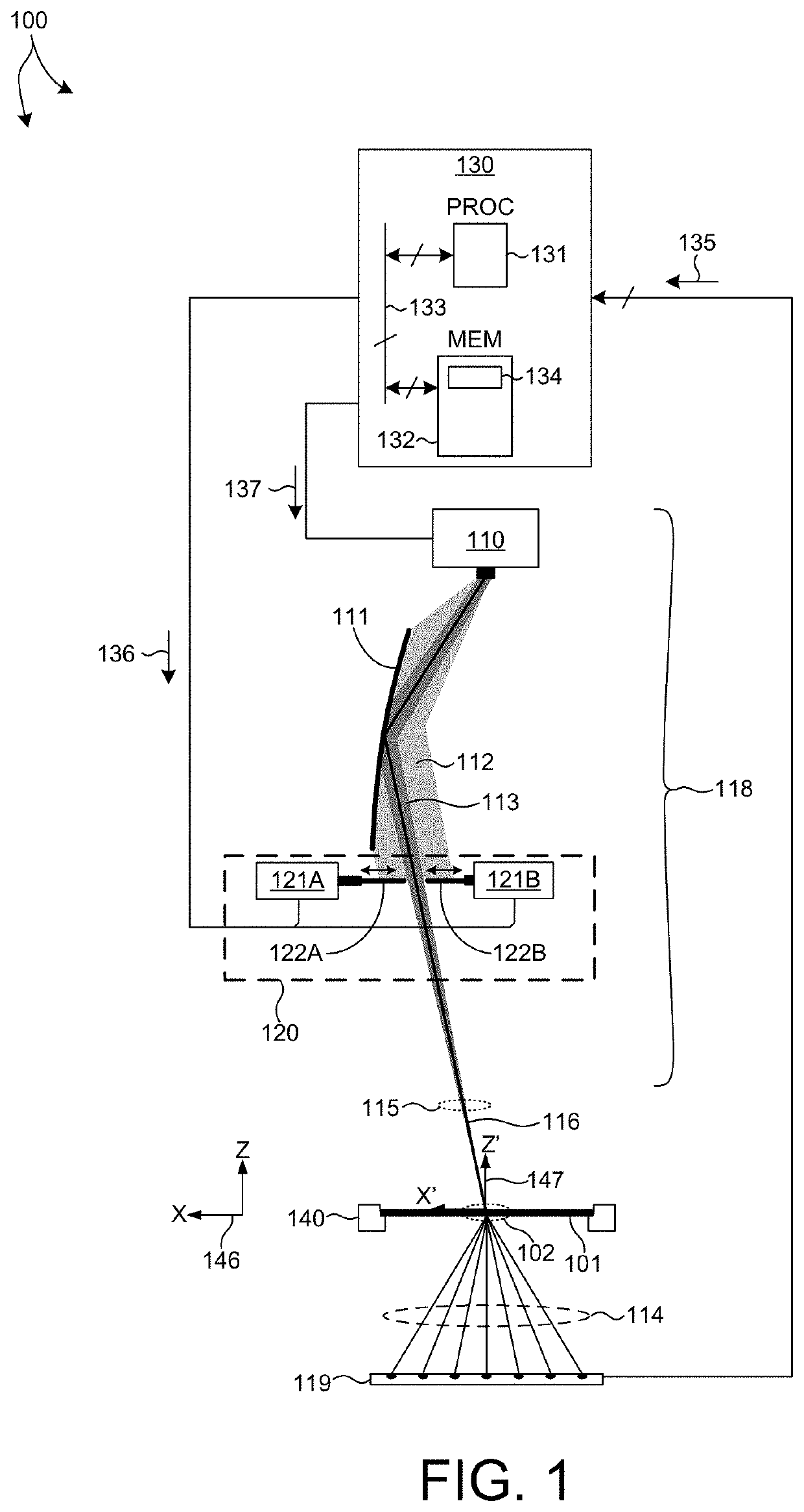
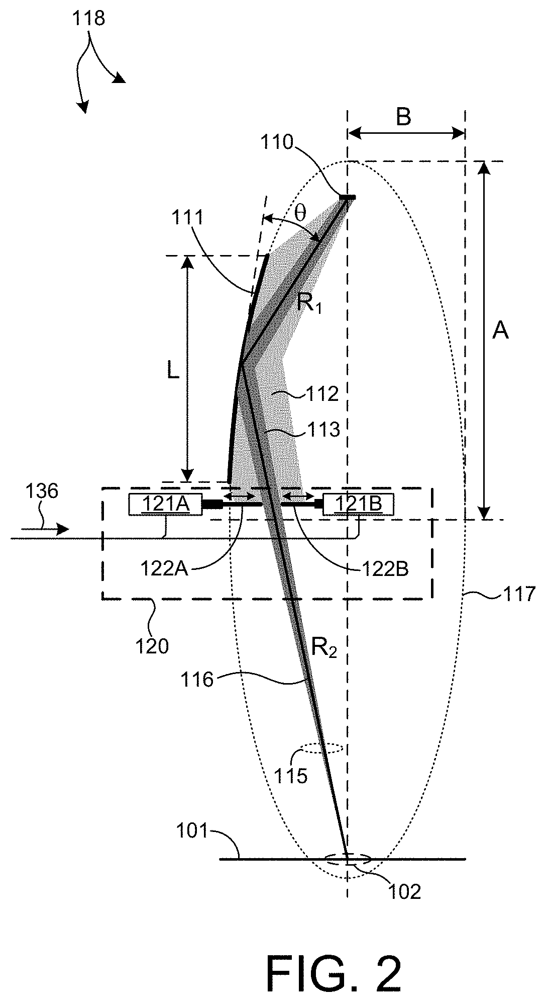
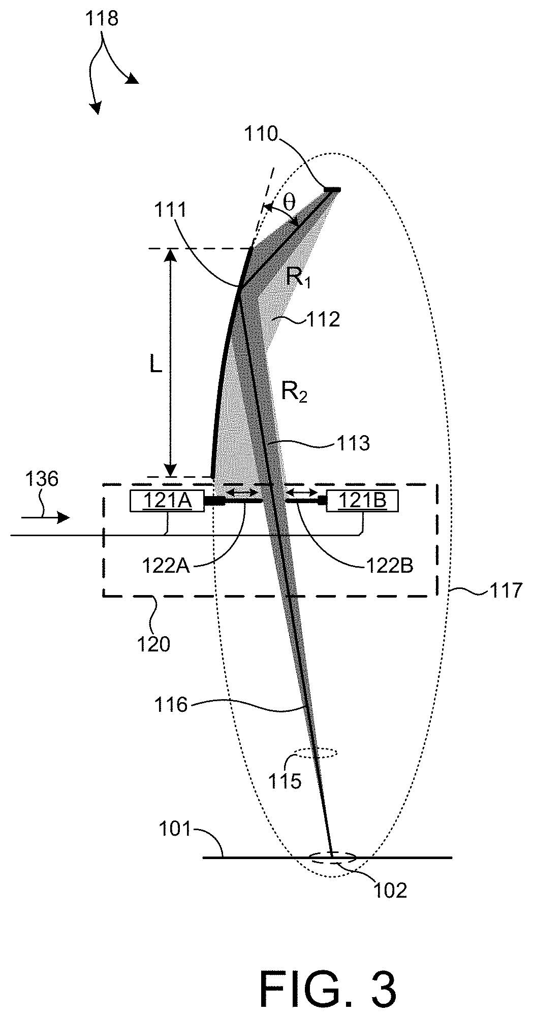
[0032]Practical T-SAXS measurements in a semiconductor manufacturing environment require measurements of different sized metrology targets with varying diffraction characteristics. In some examples, a metrology target characterized by T-SAXS measurements as described herein is located within a scribe line of a wafer under measurement. In these examples, the metrology target is sized to fit within the width of the scribe line. In some examples, the scribe line width is less than eighty micrometers. In some examples, the scribe line is less than fifty micrometers. In general, the width of the scribe lines employed in semiconductor manufacturing is trending smaller. In some examples, the metrology target characterized by T-SAXS measurements as described herein is located within an active die area of the wafer under measu...


PUM

PropertyMeasurementUnit
angles of incidenceaaaaaaaaaa
distanceaaaaaaaaaa
roughnessaaaaaaaaaa

Abstract

Methods and systems for controlling illumination beam spot size for Transmission, Small-Angle X-ray Scatterometry (T-SAXS) measurements of different sized metrology targets are described herein. An X-ray illumination optics subsystem includes one or more focusing optical elements with object and image planes at fixed locations and one or more illumination apertures or slits that independently control magnification and beam divergence. In a further aspect, the illumination source size and shape is controlled, along with magnification and beam divergence. In this manner, beam divergence and illumination spot size on a specimen are independently controlled, while maintaining constant illumination flux.

Description

CROSS REFERENCE TO RELATED APPLICATION[0001]The present application for patent claims priority under 35 U.S.C. § 119 from U.S. provisional patent application Ser. No. 62 / 441,707, filed Jan. 3, 2017, the subject matter of which is incorporated herein by reference in its entirety.TECHNICAL FIELD[0002]The described embodiments relate to x-ray metrology systems and methods, and more particularly to methods and systems for improved measurement accuracy.BACKGROUND INFORMATION[0003]Semiconductor devices such as logic and memory devices are typically fabricated by a sequence of processing steps applied to a specimen. The various features and multiple structural levels of the semiconductor devices are formed by these processing steps. For example, lithography among others is one semiconductor fabrication process that involves generating a pattern on a semiconductor wafer. Additional examples of semiconductor fabrication processes include, but are not limited to, chemical-mechanical polishing...

Claims


Application Information

Patent Timeline
Patent Type & Authority Patents(United States)
IPC IPC(8): G01N23/201
CPCG01N23/201G01N2223/1016G01N2223/6116G01N23/20008G01N23/2076G01B15/00G01N2223/05
Inventor ARTEMIEV, NIKOLAYFRIEDMANN, MICHAEL
Owner KLA CORP
Why Eureka
Try Eureka