3-d stacking semiconductor assembly having heat dissipation characteristics
a semiconductor and heat dissipation characteristic technology, applied in the field of semiconductor assemblies, can solve the problems of reducing reliability, reducing the useful life of the assembly, and affecting the performance of the devi
- Summary
- Abstract
- Description
- Claims
- Application Information
AI Technical Summary
Benefits of technology
Problems solved by technology
Method used
Image

Examples
embodiment 1
[0045]FIGS. 1-16 are schematic views showing a method of making a semiconductor assembly that includes a primary routing circuitry, a stiffener, a first device, a second device, an interconnect substrate, bonding wires and a molding compound in accordance with the first embodiment of the present invention.
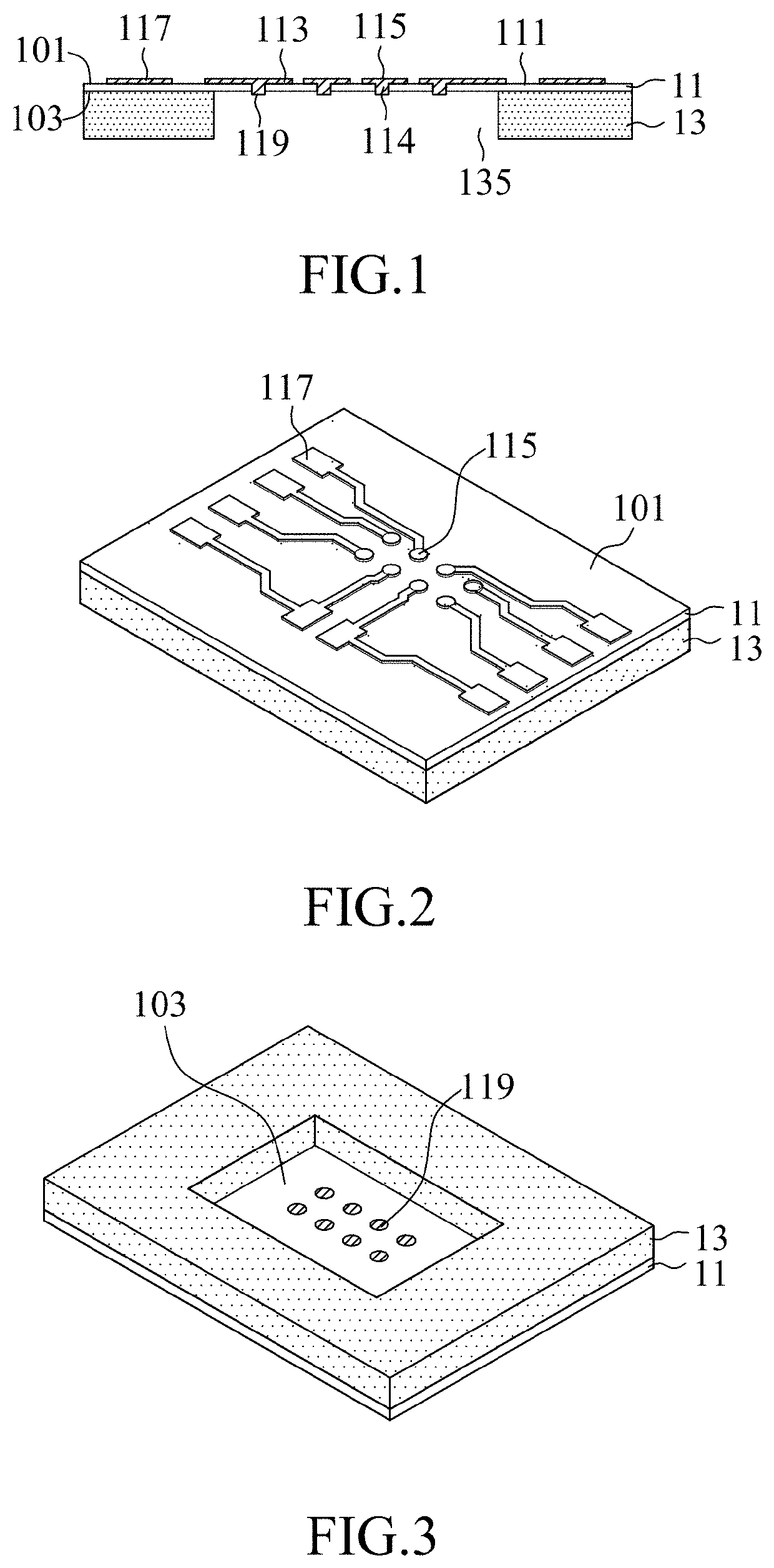
[0046]FIGS. 1, 2 and 3 are cross-sectional, top and bottom perspective views, respectively, of a primary routing circuitry 11 bonded with a stiffener 13. In this embodiment, the primary routing circuitry 11 is a multi-layered buildup circuitry and includes a dielectric layer 111 and a wiring layer 113. The dielectric layer 111 typically has a thickness of 50 microns, and can be made of epoxy resin, glass-epoxy, polyimide, or the like. The wiring layer 113 typically is made of copper and extends laterally on the dielectric layer 111 and includes conductive vias 114 extending through the dielectric layer 111. As shown in FIGS. 2 and 3, the wiring layer 113 provides first conductive p...
embodiment 2
[0055]FIGS. 20-24 are schematic views showing a method of making a semiconductor assembly in which the thermal pad has stepped peripheral edges in accordance with the second embodiment of the present invention.
[0056]For purposes of brevity, any description in Embodiment 1 is incorporated herein insofar as the same is applicable, and the same description need not be repeated.
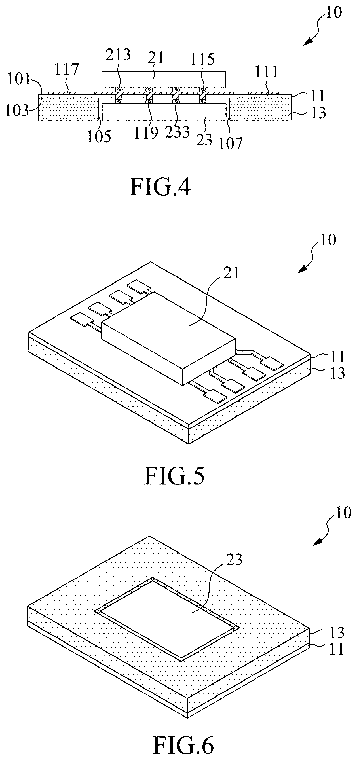
[0057]FIG. 20 is a cross-sectional view of a stacked semiconductor subassembly 10 having a primary routing circuitry 11, a stiffener 13, a first device 21, a second device 23, a passive component 24 and a metal pillar 25. In this illustration, the primary routing circuitry 11 is a multi-layered buildup circuitry and includes a dielectric layer 111 and a plurality of wiring layers 113 serially formed in an alternate fashion. The first device 21 is electrically coupled to the primary routing circuitry 11 from the first surface 101 of the primary routing circuitry 11, and the second device 23, the passive component ...
embodiment 3
[0063]FIGS. 26-33 are schematic views showing a method of making a semiconductor assembly in which the metal leads have stepped peripheral edges in accordance with the third embodiment of the present invention.
[0064]For purposes of brevity, any description in the Embodiments above is incorporated herein insofar as the same is applicable, and the same description need not be repeated.
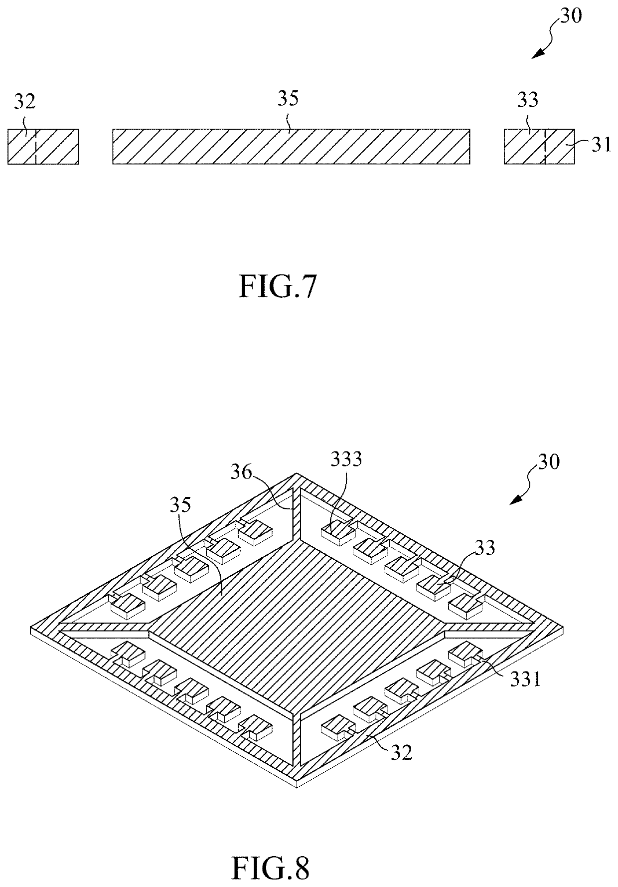
[0065]FIGS. 26 and 27 are cross-sectional and top perspective views, respectively, of a lead frame 31 having a metal frame 32, a plurality of metal leads 33 and a thermal pad 35. In this embodiment, the metal leads 33 are shaped into elongated strips parallel to each other and integrally connected to the metal frame 32 and have stepped peripheral edges. The thermal pad 35 is a thermally conductive and electrically insulating pad and located at the central area within the metal frame 32.
[0066]FIGS. 28 and 29 are cross-sectional and top perspective views, respectively, of the structure provided with a comp...
PUM
| Property | Measurement | Unit |
|---|---|---|
| thickness | aaaaa | aaaaa |
| thickness | aaaaa | aaaaa |
| elastic modulus | aaaaa | aaaaa |
Abstract
Description
Claims
Application Information
PatSnap Eureka turns technology decisions into work you can execute. Powered by our Innovation Knowledge Graph, it runs expert workflows across engineering, life sciences, materials and intellectual property. Get your review-ready output in minutes.


