LED wafer-level chip scale packaging

Inactive Publication Date: 2006-12-14
IND TECH RES INST
View PDF11 Cites 101 Cited by
  • Summary
  • Abstract
  • Description
  • Claims
  • Application Information

AI Technical Summary

Benefits of technology

[0012] In view of the foregoing, it is an object of the present invention to provide the method for and the structure of the light emitting diode (LED) wafer-le

Problems solved by technology

As the LED becomes more high-power, more heat is therefore generated, which disadvantageously leads to worsened characteristics, declined intensity, and even burnt-out device.
Conventionally, the LED packaging seldom concerns the heat dissipation, which is

Method used


Image

  • LED wafer-level chip scale packaging
  • LED wafer-level chip scale packaging
  • LED wafer-level chip scale packaging

Examples


Embodiment Construction

[0022] The detailed description of the present invention will be discussed in the following embodiments, which are not intended to limit the scope of the present invention, but can be adapted for other applications. While drawings are illustrated in details, it is appreciated that the quantity of the disclosed components may be greater or less than that disclosed, except expressly restricting the amount of the components.

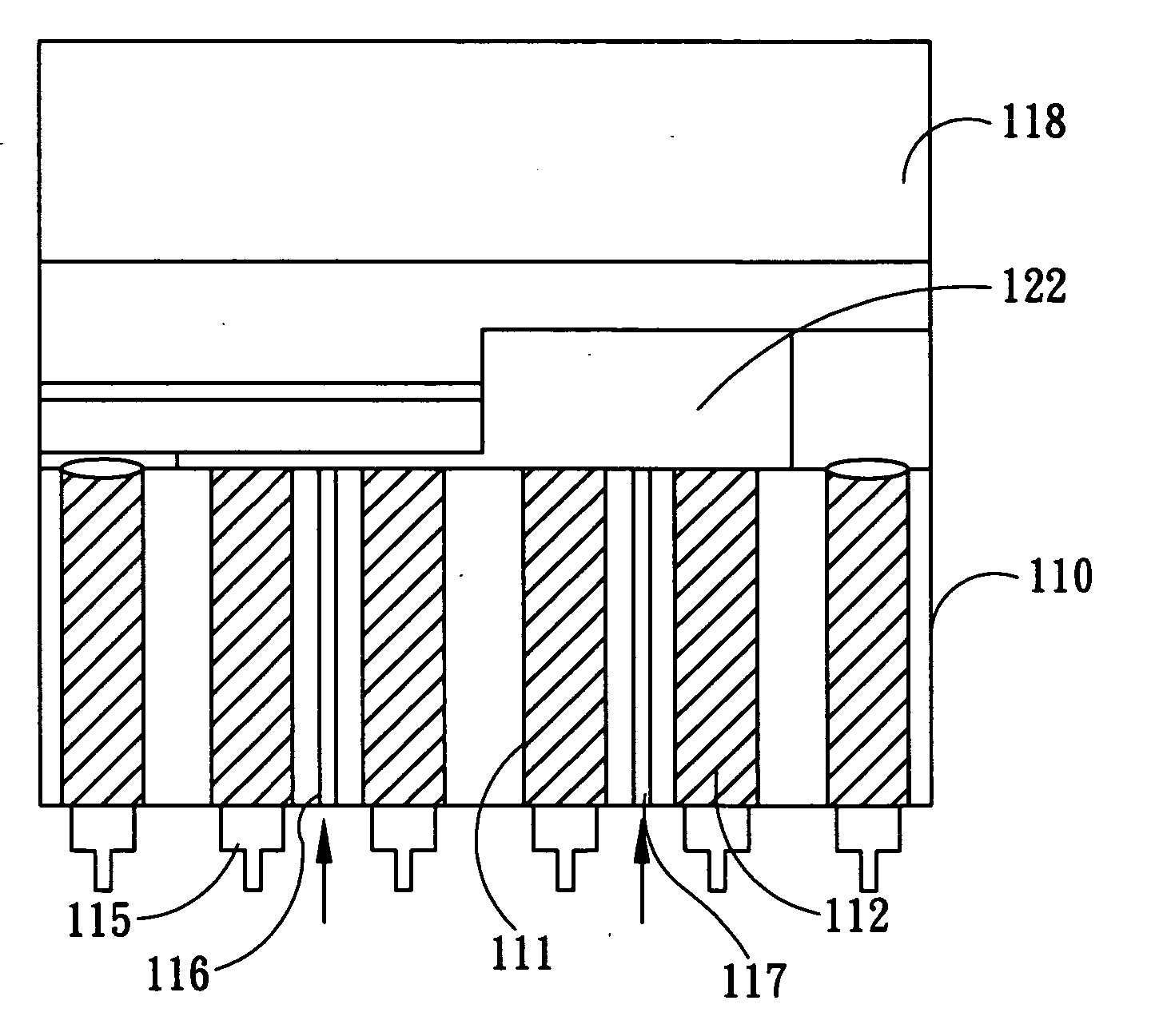
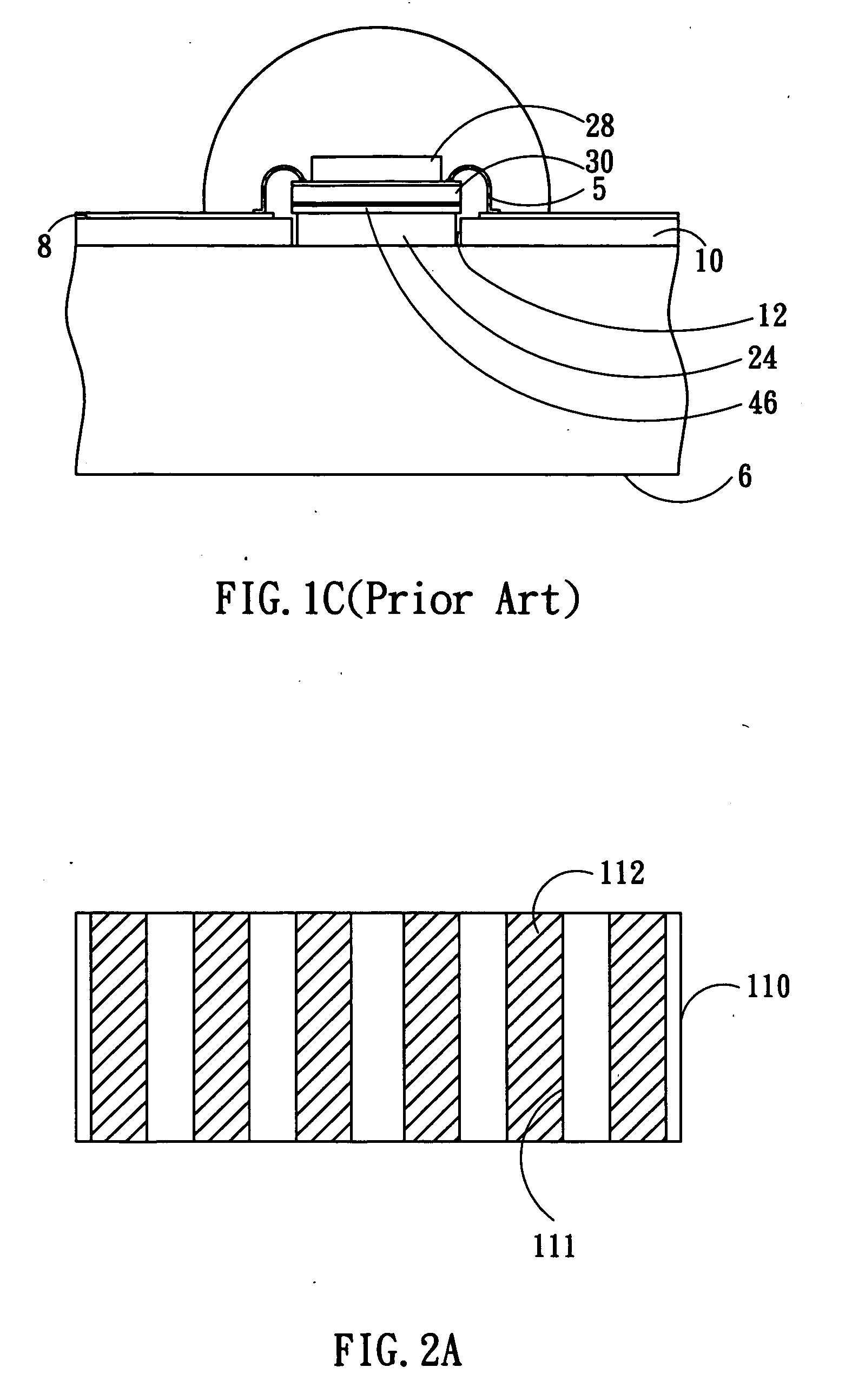
[0023]FIG. 2A to FIG. 2E schematically illustrate the cross-sectional views of the light emitting diode (LED) wafer-level chip scale packaging (WL-CSP) according to one embodiment of the present invention. As showing in FIG. 2A, a carrier substrate 110, which is also known as submount or substrate, is provided, and at least one through hole or thermal via 111 is formed through the carrier substrate 110. Usually, more than one through hole 111 is formed to enhance heat conduction. The through holes 111 could be made by using conventional drilling technique such as e...


PUM


Abstract

A structure of light emitting diode (LED) wafer-level chip scale packaging (WL-CSP) is disclosed. The process of making the same is also provided in this invention. The LED CSP utilizes the through hole metal filling to enhance heat conduction between the LED die and its carrier substrate. The CSP structure is achieved by bonding pre-processed through-hole-filling carrier substrate against the flip-chip LED wafer.

Description

BACKGROUND OF THE INVENTION [0001] 1. Field of the Invention [0002] The present invention generally relates to light emitting diode (LED) packaging, and more particularly to light emitting diode (LED) wafer-level chip scale packaging (WL-CSP) for enhancing heat conduction. [0003] 2. Description of the Prior Art [0004] Light emitting diode (LED) is a device that transforms electric power into light source. Compared with conventional light sources, the LED has advantages of low input voltage, low power consumption, and quick response time. Furthermore, the LED has other beneficial characteristics, such as light weight, low cost to manufacture, and capability of mass production. Accordingly, the LED has become an indispensable element in the modern life, especially in the electronic, communication, and consumer products fields. [0005] One of the main purposes of semiconductor packaging is to protect the circuit chip from being damaged physically or chemically, ensuring the proper funct...

Claims


Application Information

Patent Timeline
IPC IPC(8): H01L33/00H01L33/38H01L33/48H01L33/62H01L33/64
CPCH01L33/486H01L33/62H01L33/641H01L33/642H01L2224/16H01L2224/48091H01L2924/12041H01L2924/00012H01L2224/0554H01L2224/05568H01L2224/05573H01L2924/00014H01L2224/05599H01L2224/0555H01L2224/0556
Inventor TAIN, RA-MINLO, WEI-CHUNGSHEN, LI-CHENG
Owner IND TECH RES INST
Why Eureka
Try Eureka